Method for making simulated fingerprint

A production method and technology of fingerprints, which are applied in the directions of acquiring/arranging fingerprints/palmprints, detecting live finger shapes, and collecting printed images, can solve the problems of low recognition rate, poor image quality, and recognition rate that cannot meet the requirements, and achieve Guaranteed yield rate, improved recognition rate, and high accuracy

Active Publication Date: 2020-11-17
SHENZHEN GOODIX TECH CO LTD
View PDF7 Cites 0 Cited by
  • Summary
  • Abstract
  • Description
  • Claims
  • Application Information

AI Technical Summary

Problems solved by technology

[0006] However, the image quality of the current simulated fingerprints is poor, so the recognition rate of the produced simulated fingerprints is low when evaluating the capacitive fingerprint sensor, which leads to the fact that when the current simulated fingerprint is used to evaluate the capacitive fingerprint sensor, the recognition rate cannot meet the requirements. And further lead to the deviation between the true rejection rate and the false recognition rate, and finally lead to the current emulation fingerprint cannot correctly evaluate the product performance of the capacitive fingerprint sensor, hindering the improvement of the product performance of the capacitive fingerprint sensor, and using the current emulation fingerprint to When the capacitive fingerprint sensor is tested in batches, the yield rate of the product cannot be guaranteed

Method used


Image

  • Method for making simulated fingerprint
  • Method for making simulated fingerprint
  • Method for making simulated fingerprint

Examples


Embodiment 1

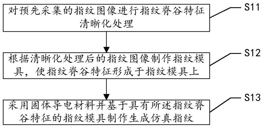
[0056] This embodiment provides a schematic flow chart of an embodiment of a method for making a simulated fingerprint, as figure 1 shown, which includes:

[0057] S11. Perform fingerprint ridge-valley feature clarification processing on the pre-collected fingerprint image.

[0058] In this embodiment, fingerprint images can be formed by pre-collecting fingerprints by the following methods:

[0059] (1) After dipping the colored ink pad on the finger, press it on the paper, and finally scan the fingerprint image through the scanner; or,

[0060] (2) collecting fingerprints through optical sensors, and obtaining fingerprint images by sensing the brightness and darkness of light reflected by fingerprints; or,

[0061] (3) After using graphite powder to display the finger print on the object, carry out image acquisition to obtain the fingerprint image on the object.

[0062] In order to ensure that the produced simulated fingerprint has a relatively high similarity with the re...

Embodiment 2

[0092] The present invention provides a schematic flow chart of an embodiment of a method for obtaining a fingerprint mold through a printed circuit board, as shown in image 3 shown, which includes:

[0093] S21. Convert the fingerprint image after clearing processing into a fingerprint image recognizable by the production control software of the printed circuit board factory and output the circuit board description file;

[0094] In this embodiment, the sharpened fingerprint image may be a fingerprint image that has undergone ridge-to-valley conversion.

[0095] In this embodiment, for example, the Allegro tool of Cadence Electronic Technology Co., Ltd. can be used to convert the image into a fingerprint image that can be recognized by the printed circuit board production control software.

[0096] In this embodiment, the fingerprint image can also be transformed into a fingerprint image recognizable by the printed circuit board production control software in other ways, an...

Embodiment 3

[0102] The present invention also provides a schematic flow chart of another embodiment of a method for obtaining a fingerprint mold by printing a printed circuit board, as shown in Figure 4 shown, which includes:

[0103] S31. Printing the sharpened fingerprint image on a film;

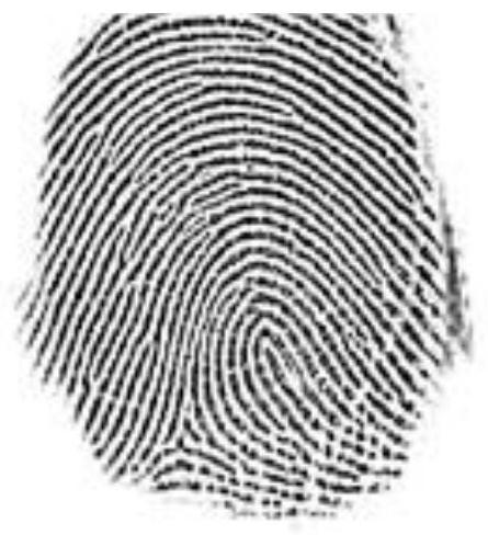
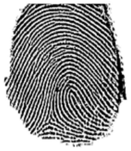
[0104] In order to facilitate subsequent photosensitive processing, transparent and translucent films can be used. In this embodiment, transparent film is taken as an example. After printing the fingerprint image that has undergone sharpening and ridge-valley conversion on the film, the ridge-valley features of the fingerprint are attached to the film, and the ridge features of the fingerprint are black. Printing on the transparent film The black part will be opaque; the fingerprint valley feature is white, and the white part will be transparent after printing on the transparent film, as shown in Figure 5(b).

[0105] S32. Paste the film printed with the sharpened fingerprint image on the printed ...


PUM


Abstract

The invention provides a method for making a simulated fingerprint, comprising: performing fingerprint ridge-valley feature clearing processing on a pre-collected fingerprint image, making a fingerprint mold according to the fingerprint image after clearing processing, so that the fingerprint ridge-valley feature is formed on the fingerprint mold ; Using solid conductive material or liquid conductive material and based on the fingerprint mold with the characteristics of the fingerprint ridges and valleys to generate simulated fingerprints. The simulated fingerprint produced by the method for making the simulated fingerprint provided by the embodiment of the present invention has obvious ridge and valley features, which improves the recognition rate of the simulated fingerprint. When the simulated fingerprint is used to evaluate the capacitive fingerprint sensor, the recognition rate meets the requirements, and the evaluation results are rejected. The accuracy of the rate and false recognition rate is high, which is conducive to improving the performance of the capacitive fingerprint sensor, and can ensure the yield rate of the product during batch testing.

Description

technical field [0001] The embodiment of the present invention relates to the field of fingerprint identification, and in particular to a method for making a simulated fingerprint. Background technique [0002] Due to the characteristics of uniqueness and stability of fingerprints, identity recognition can be realized accordingly. The fingerprint sensor is a key device to realize automatic fingerprint collection, and the capacitive fingerprint sensor has been widely used in smart terminals. [0003] The principle of the capacitive fingerprint sensor is on a "flat plate" integrated with thousands of semiconductor devices. Fingers are pasted on it to form the other side of the capacitor. Since the finger plane is uneven, the convex points and concave points correspond to each other. Fingerprint ridge features and fingerprint valley features lead to different actual distances from the touch plate, resulting in different capacitance values. According to this principle, the coll...

Claims


Application Information

Patent Timeline
Patent Type & Authority Patents(China)
IPC IPC(8): G06K9/00
CPCG06V40/1306G06V40/1359G06V40/1382
Inventor 陈文斌杨旺旺余旖王玉栋李丹
Owner SHENZHEN GOODIX TECH CO LTD
Why Eureka
Try Eureka