Display panel and manufacturing method thereof, and display apparatus

A display panel and display area technology, which is applied in semiconductor/solid-state device manufacturing, static indicators, instruments, etc., can solve the problems of strong graininess and poor display effect, reduce graininess, increase coverage, and weaken jaggies Effect

Active Publication Date: 2017-08-25
BOE TECH GRP CO LTD +1
View PDF3 Cites 16 Cited by
  • Summary
  • Abstract
  • Description
  • Claims
  • Application Information

AI Technical Summary

Problems solved by technology

[0004] In order to solve the problem in the related art that the image displayed at the edge of the display area has a strong graininess an

Method used


Image

  • Display panel and manufacturing method thereof, and display apparatus
  • Display panel and manufacturing method thereof, and display apparatus
  • Display panel and manufacturing method thereof, and display apparatus

Examples


Embodiment Construction

[0040] In order to make the object, technical solution and advantages of the present invention clearer, the implementation manner of the present invention will be further described in detail below in conjunction with the accompanying drawings.

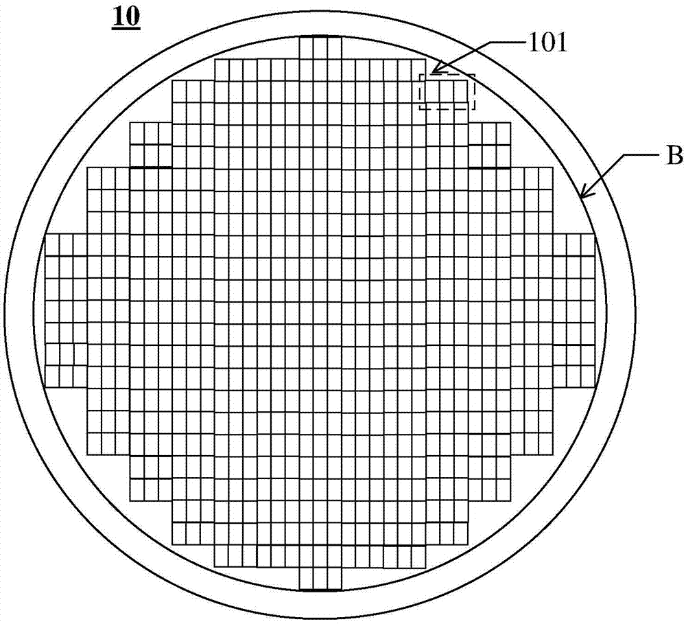
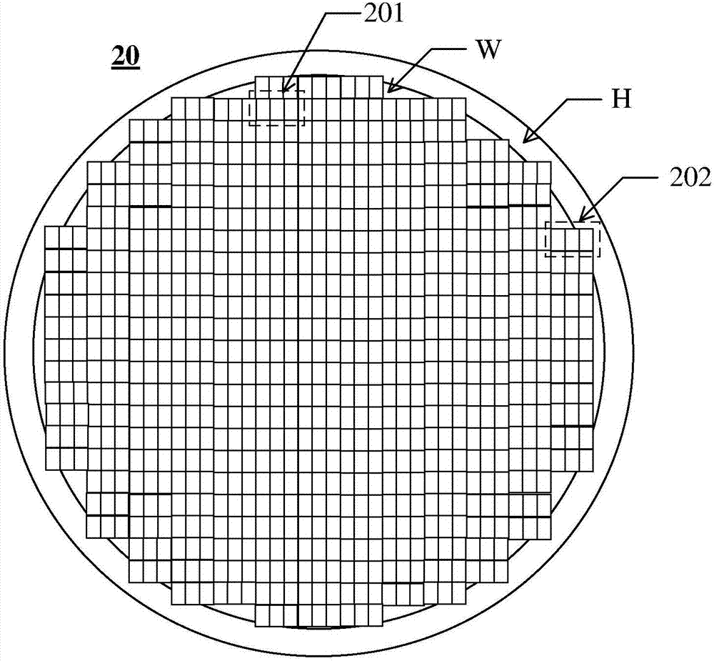
[0041] An embodiment of the present invention provides a display panel 20, which may be an Active Matrix Organic Light Emitting Diode (English: Active Matrix Organic Light Emitting Diode; AMOLED for short) display panel, such as figure 2 As shown, the display panel 20 has a display area W and a non-display area H, and the display panel 20 includes:

[0042] The base substrate and the display unit arranged on the base substrate, the display unit includes a plurality of pixels and a pixel driving circuit, and the pixel driving circuit is used to drive the plurality of pixels to emit light.

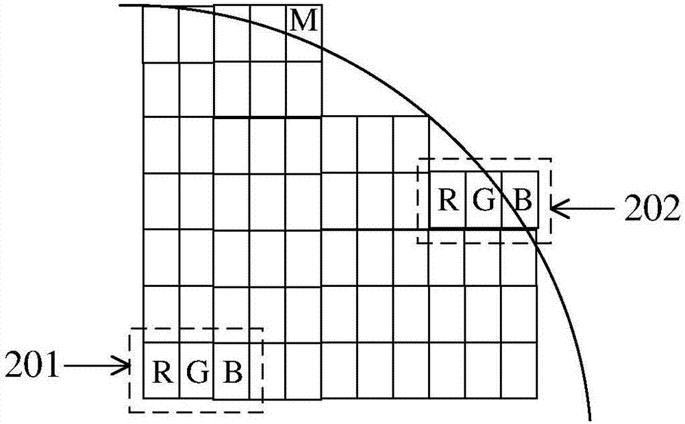
[0043] Wherein, the plurality of pixels includes a plurality of first pixels 201 and a plurality of second pixels 202, the plurality of first pixel...


PUM


Abstract

The invention discloses a display panel and a manufacturing method thereof, and a display apparatus and belongs to the display technology field. The display panel possesses a display area and a non-display area. The display panel comprises a substrate and a display unit arranged on the substrate. The display unit comprises a plurality of pixels and a pixel driving circuit. The pixel driving circuit is used for driving the plurality of pixels to shine. The plurality of pixels comprises a plurality of first pixels and a plurality of second pixels. The plurality of first pixels are arranged in a first configuration area in an array mode. The plurality of second pixels are arranged in a periphery of the first configuration area. Each second pixel is simultaneously located in a second configuration area and a third configuration area. The first configuration area and the second configuration area are located in the display area. The third configuration area is located in the non-display area. In a correlation technology, granular sensation of an image displayed at an edge position of the display area is high and a display effect is poor. By using the display panel, the method and the apparatus of the invention, the above problems are solved. The method of the invention is used for manufacturing of the display panel.

Description

technical field [0001] The present invention relates to the field of display technology, in particular to a display panel, a manufacturing method thereof, and a display device. Background technique [0002] With the development of display technology, Organic Light Emitting Diode (English: Organic Light Emitting Diode; abbreviation: OLED), as a current-type light-emitting device, has become more and more popular due to its characteristics such as self-illumination, fast response, and wide viewing angle. It is widely used in the field of high-performance display. [0003] For example, OLED can be applied in the field of smart wearable display, and the display panel of the smart wearable device is generally a non-rectangular display panel, such as a circular display panel. In the related art, OLED display panels generally use rectangular pixels, such as figure 1 As shown, when the circular OLED display panel 10 uses rectangular pixels 101, the edges of the rectangular pixels ...

Claims


Application Information

Patent Timeline
IPC IPC(8): G09G3/3291G09G3/3208H01L27/32H01L51/56
CPCG09G3/3208G09G3/3291H10K59/353H10K71/00G09G3/3233G09G2310/0232G09G2300/0819G09G2300/0861G09G2300/0842G09G2320/0233H10K59/88G09G2300/08
Inventor 刘庭良黄炜赟龙跃董向丹王杨
Owner BOE TECH GRP CO LTD
Why Eureka
Try Eureka