Display device and fingerprint identification method thereof and electronic device

A technology for display device and fingerprint identification, which is applied in the field of electronic equipment and display devices, can solve problems affecting the accuracy of fingerprint identification sensor fingerprint identification, etc., and achieve the effect of improving the accuracy of fingerprint identification

Active Publication Date: 2017-09-01
SHANGHAI TIANMA MICRO ELECTRONICS CO LTD
View PDF6 Cites 44 Cited by
  • Summary
  • Abstract
  • Description
  • Claims
  • Application Information

AI Technical Summary

Problems solved by technology

[0003] In the existing display device with fingerprint identification function, when the light emitted by the fingerprint identification light source is reflected by the finger, it will be irradiated on a plurality of fingerprint identification sensors, so that each fingerprint identification sensor receives the fingerprint signal corresponding to its position, It also receives crosstalk signals from other locations, which affects the accuracy of fingerprint recognition by the fingerprint recognition sensor

Method used


Image

  • Display device and fingerprint identification method thereof and electronic device
  • Display device and fingerprint identification method thereof and electronic device
  • Display device and fingerprint identification method thereof and electronic device

Examples


Embodiment Construction

[0069] In order to make the purpose, technical solutions and advantages of the present invention clearer, the technical solutions of the present invention will be clearly and completely described through implementation with reference to the accompanying drawings in the embodiments of the present invention. Obviously, the described embodiments are the embodiment of the present invention. Some, but not all, embodiments. Based on the embodiments of the present invention, all other embodiments obtained by persons of ordinary skill in the art without making creative efforts belong to the protection scope of the present invention.

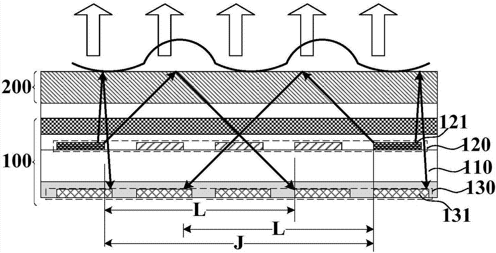
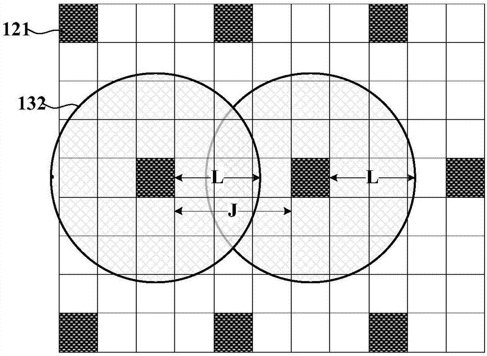
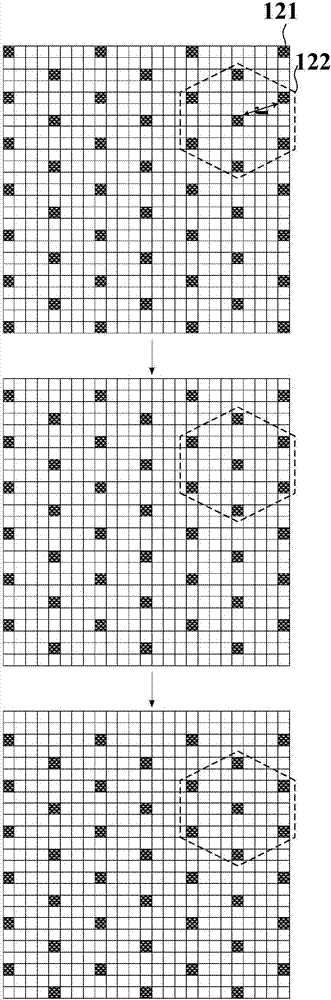
[0070] Such as Figure 1A As shown, it is a schematic diagram of a display device provided by an embodiment of the present invention, Figure 1B for Figure 1A A partial top view of the display device shown, Figure 1C for Figure 1A Schematic diagram of scanning in the fingerprint recognition stage of the shown display device. The display device provi...


PUM


Abstract

An embodiment of the invention discloses a display device and a fingerprint identification method thereof and an electronic device. The display device comprises a display panel and a cover plate arranged on the display panel. The display panel comprises an array substrate, an organic light-emitting layer arranged at one side, facing to the cover plate, of the array substrate, and a fingerprint identification array. The organic light-emitting layer comprises a plurality of organic light-emitting structures. A first surface, away from the array substrate, of the cover plate is a light output surface of the display device. In the fingerprint identification stage, the plurality of organic light-emitting structures realize displacement and light emitting according to a first light-emitting dot matrix; the distance between any two adjacent organic light-emitting structures in the first light-emitting dot matrix is larger than or equal to minimum no-crosstalk distance; and the minimum no-crosstalk distance is the maximum radius of a coverage area formed on the fingerprint identification array when light emitted by any one organic light-emitting structure is reflected by the first surface of the cover plate. Fingerprint identification units are not influenced by crosstalk of other organic light-emitting structures, so that fingerprint recognition accuracy of the display device can be improved.

Description

technical field [0001] Embodiments of the present invention relate to display technologies, and in particular to a display device, a fingerprint identification method thereof, and electronic equipment. Background technique [0002] Fingerprints are inherent to each person and are unique. With the development of technology, a variety of display devices with fingerprint recognition functions appear on the market, such as mobile phones, tablet computers, and smart wearable devices. In this way, before operating the display device with the fingerprint recognition function, the user only needs to touch the fingerprint recognition sensor of the display device with a finger to perform authority verification, which simplifies the authority verification process. [0003] In the existing display device with fingerprint identification function, when the light emitted by the fingerprint identification light source is reflected by the finger, it will be irradiated on a plurality of fing...

Claims


Application Information

Patent Timeline
Patent Type & Authority Applications(China)
IPC IPC(8): G06K9/00
CPCG06V40/1324G06F3/0416G06F3/0421G06V40/1318H10K59/65G06F3/0412G06V40/1306G06V40/1329G06V40/1359H10K50/84H10K50/805H10K59/40H10K59/122
Inventor 曾洋张卿王丽花谢亮杜凌霄丁洪柴慧平杨康姚绮君
Owner SHANGHAI TIANMA MICRO ELECTRONICS CO LTD
Why Eureka
Try Eureka