A method and cmos device for adjusting the threshold of high-k metal gate cmos device

A metal gate and device technology, which is applied in the manufacturing of semiconductor devices, electric solid-state devices, semiconductor/solid-state devices, etc., can solve the problems of poor controllability, channel process damage, and small thickness distinction range, and achieves a large thickness controllable range. , the effect of reducing process damage and integrating process is simple

Active Publication Date: 2019-11-12
INST OF MICROELECTRONICS CHINESE ACAD OF SCI +1
View PDF4 Cites 0 Cited by
  • Summary
  • Abstract
  • Description
  • Claims
  • Application Information

AI Technical Summary

Problems solved by technology

[0004] The embodiment of the present application provides a method for adjusting the threshold of a high-K metal gate CMOS device and a CMOS device, which solves the problem of small thickness distinction range, poor controllability, and proximity to the interface in the threshold adjustment process of high-K metal gate CMOS devices in the prior art. Technical problems that are likely to cause process damage to the channel

Method used


Image

  • A method and cmos device for adjusting the threshold of high-k metal gate cmos device
  • A method and cmos device for adjusting the threshold of high-k metal gate cmos device
  • A method and cmos device for adjusting the threshold of high-k metal gate cmos device

Examples


Embodiment 1

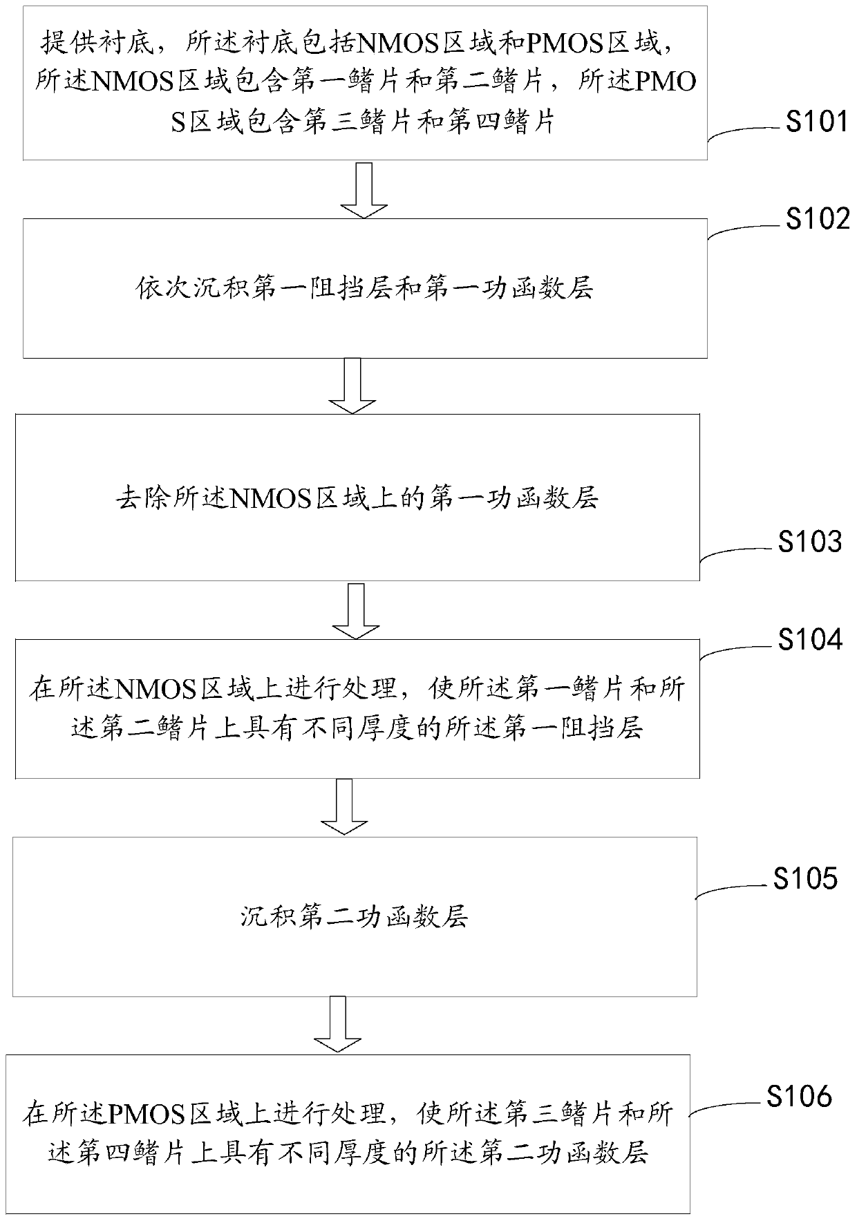
[0048] In this embodiment, a method for adjusting the threshold of a high-K metal gate CMOS device is provided, such as figure 1 shown, including:

[0049] S101, providing a substrate, where the substrate includes an NMOS region and a PMOS region, the NMOS region includes a first fin and a second fin, and the PMOS region includes a third fin and a fourth fin;

[0050] S102, sequentially depositing a first barrier layer and a first work function layer;

[0051] S103, removing the first work function layer on the NMOS region;

[0052] S104, performing processing on the NMOS region, so that the first barrier layer has different thicknesses on the first fin and the second fin;

[0053] S105, depositing a second work function layer;

[0054] S106. Perform processing on the PMOS region, so that the third fin and the fourth fin have the second work function layer with different thicknesses.

[0055] Below, combine Figure 1-7 To introduce in detail the detailed steps of the method...

Embodiment 2

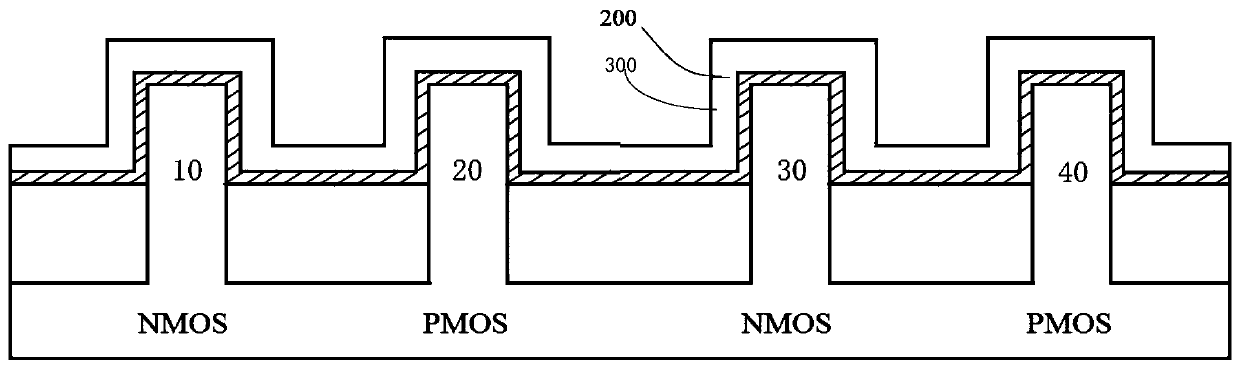
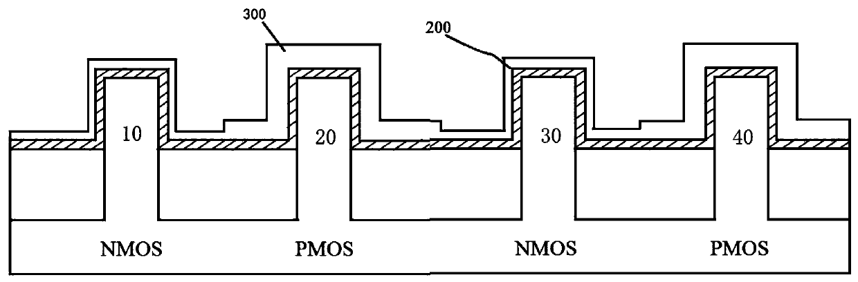
[0092] In this embodiment, a CMOS device is provided, such as Figure 6 shown, including:

[0093] A substrate 100, the substrate 100 includes an NMOS area and a PMOS area, the NMOS area includes the first fin 10 and the second fin 30, and the PMOS area includes the third fin 20 and the fourth fin 40;

[0094] The first barrier layer 200 is located on the NMOS region and the PMOS region, and the first barrier layer 200 has different thicknesses on the first fin 10 and the second fin 30;

[0095] A first work function layer 300, the first work function layer 300 is located on the first barrier layer 200 of the PMOS region;

[0096] The second work function layer 400, the second work function layer 400 is located on the first barrier layer 200 in the NMOS region and on the first work function layer 300 in the PMOS region, wherein the second work function layer 400 The third fin 20 and the fourth fin 40 have the second work function layer 400 with different thicknesses.

[009...


PUM


Abstract

The invention discloses a method for adjusting a threshold of a high K metal gate CMOS device and a CMOS device, and the method comprises the steps: a substrate is provided, an NMOS region comprises a first fin and a second fin, and a PMOS region comprises a third fin and a fourth fin; a first barrier layer and a first work function layer are deposited in sequence; the first work function layer on the NMOS region is removed; the first fin and the second fin have the first barrier layers with different thickness; a second work function layer is deposited; and the third fin and the fourth fin have the second work function layers with different thickness. According to the invention, the method and the device are used for solving technical problems that the technology for adjusting the threshold of the high K metal gate CMOS device in the prior art has small thickness differentiate range and poor controllability, and closing an interface is easy to cause technical damage to a channel. The controllable range of the thickness of a threshold adjusting and controlling layer is improved, and the technical effect of technical damage to the channel is reduced.

Description

technical field [0001] The invention relates to the technical field of semiconductor integration, in particular to a method for adjusting the threshold of a high-K metal gate CMOS device and the CMOS device. Background technique [0002] The existing method for adjusting the threshold of high-K metal gate CMOS devices is: first deposit barrier layer and deposit PMOS work function layer (PMOS WFL) on the metal gate of NMOS and PMOS, and then remove PMOS WFL in NMOS area and adjust the thickness of barrier layer in NMOS area To adjust the NMOS threshold, change the thickness of the PMOS WFL in the PMOS region to adjust the PMOS threshold; and then deposit the NMOS work function layer (NMOS WFL). [0003] Since the thickness adjustment of the metal gate work function threshold of NMOS and PMOS in the existing method is based on the corrosion of the barrier layer and the TiNx-based material of the PMOS WFL, the thickness range is small, the controllability is poor, and the adjac...

Claims


Application Information

Patent Timeline
Patent Type & Authority Patents(China)
IPC IPC(8): H01L21/8238H01L27/092
CPCH01L21/823821H01L21/823842H01L21/82385H01L27/0924
Inventor 殷华湘张青竹赵超叶甜春
Owner INST OF MICROELECTRONICS CHINESE ACAD OF SCI
Why Eureka
Try Eureka