Method for adjusting threshold of high-K metal gate CMOS device and CMOS device

A metal gate and device technology, applied in the field of semiconductor integration, can solve the problems of channel process damage, poor controllability, inaccurate corrosion thickness of barrier layer and work function layer materials, etc., to reduce process damage, large controllable range, Integrate the effect of a simple process

Inactive Publication Date: 2020-05-08
宿州市高智信息科技有限公司
View PDF0 Cites 0 Cited by
  • Summary
  • Abstract
  • Description
  • Claims
  • Application Information

AI Technical Summary

Problems solved by technology

[0005] The embodiment of the present application provides a method for adjusting the threshold of a high-K metal gate CMOS device and a CMOS device, which solves the inaccurate corrosion thickness of barrier layer and work function layer materials existing in the threshold adjustment process of high-K metal gate CMOS devices in the prior art, The controllability is poor, the device threshold adjustment is uncontrollable, and the technical problems of the adjacent interface are easy to cause process damage to the channel

Method used


Image

  • Method for adjusting threshold of high-K metal gate CMOS device and CMOS device
  • Method for adjusting threshold of high-K metal gate CMOS device and CMOS device

Examples


Embodiment 1

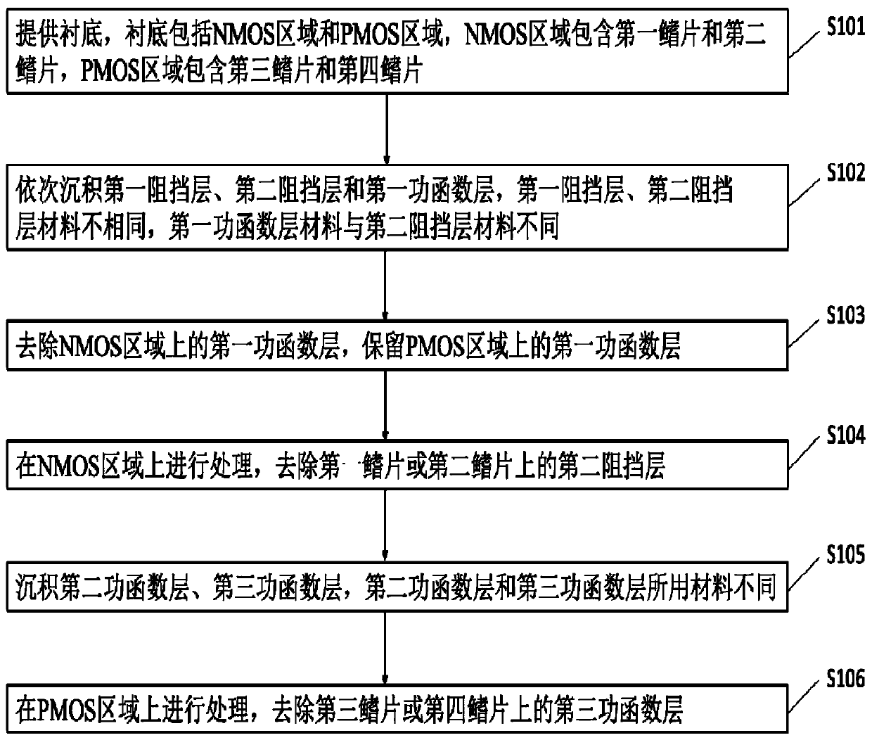
[0042] In this embodiment, a method for adjusting the threshold of a high-K metal gate CMOS device is provided, such as figure 1 shown, including:

[0043] Step S101, providing a substrate.

[0044] The substrate includes an NMOS area and a PMOS area, the NMOS area includes a first fin and a second fin, and the PMOS area includes a third fin and a fourth fin.

[0045] In the embodiment of the present application, an isolation layer / high-k dielectric layer may be disposed on the fin of the substrate.

[0046] Step S102, depositing a first barrier layer, a second barrier layer and a first work function layer in sequence.

[0047] The materials of the first barrier layer and the second barrier layer are different, and respectively include one of the following materials: TiN, TaN, TiNSi.

[0048] The first work function layer includes at least one or a combination of the following materials: TiN, TaN, TiNx, TaNx, TiNSi, and the material of the first work function layer is diffe...

Embodiment 2

[0074] In this embodiment, a CMOS device is provided, including:

[0075] a substrate, the substrate includes an NMOS region and a PMOS region, the NMOS region includes a first fin and a second fin, and the PMOS region includes a third fin and a fourth fin;

[0076] a first barrier layer located on the NMOS region and the PMOS region;

[0077] The second barrier layer is located only on the first fin region of the NMOS region and on the first barrier layer of the PMOS region, and the materials used for the first barrier layer and the second barrier layer are different;

[0078] a first work function layer, the first work function layer is located on the second barrier layer in the PMOS region, and the material of the first work function layer is different from the material of the second barrier layer;

[0079] a second work function layer located on the first barrier layer in the NMOS region, the second barrier layer and the first work function layer in the PMOS region;

[0...


PUM


Abstract

The invention discloses a method for adjusting a threshold of a high-K metal gate CMOS device and a CMOS device, and the method comprises: providing a substrate which comprises an NMOS region and a PMOS region, wherein the NMOS region comprises a first fin and a second fin, and the PMOS region comprises a third fin and a fourth fin; sequentially depositing a first barrier layer, a second barrier layer and a first work function layer, wherein the first barrier layer and the second barrier layer are made of different materials, and the first work function layer and the second barrier layer are made of different materials; removing the first work function layer on the NMOS region; processing on the NMOS region, and removing the second barrier layer on the first fin or the second fin; depositing a second work function layer and a third work function layer, wherein the second work function layer and the third work function layer are made of different materials; and processing on the PMOS region, and removing the third work function layer on the third fin or the fourth fin.

Description

technical field [0001] The invention relates to the technical field of semiconductor integration, in particular to a method for adjusting the threshold of a high-K metal gate CMOS device and the CMOS device. Background technique [0002] The existing method for adjusting the threshold of high-K metal gate CMOS devices is: first deposit barrier layer and deposit PMOS work function layer (PMOS WFL) on the metal gate of NMOS and PMOS, and then remove PMOS WFL in NMOS area and adjust the thickness of barrier layer in NMOS area To adjust the NMOS threshold, change the thickness of the PMOS WFL in the PMOS region to adjust the PMOS threshold; and then deposit the NMOS work function layer (NMOS WFL). [0003] Another prior art is to adjust the NMOS threshold by adjusting the thickness of the metal gate barrier layer in the NMOS region, and adjust the PMOS threshold by adjusting the thickness of the NMOS WFL work function layer in the PMOS region. [0004] However, in the above exi...

Claims


Application Information

Patent Timeline
Patent Type & Authority Applications(China)
IPC IPC(8): H01L27/092H01L21/8238
CPCH01L21/823814H01L21/823821H01L21/823857H01L27/0922
Inventor 程元伟郑淑云刘翰林
Owner 宿州市高智信息科技有限公司
Why Eureka
Try Eureka