
CMOS device and method for adjusting threshold value of CMOS device

A device and threshold technology, applied in semiconductor devices, electrical solid state devices, semiconductor/solid state device manufacturing, etc., can solve problems such as channel process damage and poor controllability

Active Publication Date: 2018-09-07
INST OF MICROELECTRONICS CHINESE ACAD OF SCI
View PDF3 Cites 1 Cited by
  • Summary
  • Abstract
  • Description
  • Claims
  • Application Information

AI Technical Summary

Problems solved by technology

[0004] The main purpose of the present invention is to provide a CMOS device and a method for adjusting the threshold of the CMOS device, so as to solve the problem that the threshold adjustment process of the CMOS device in the prior art has poor controllability and the process damage to the channel is easy to be caused near the interface

Method used


Image

  • CMOS device and method for adjusting threshold value of CMOS device
  • CMOS device and method for adjusting threshold value of CMOS device
  • CMOS device and method for adjusting threshold value of CMOS device

Examples


Embodiment Construction

[0025] It should be noted that, in the case of no conflict, the embodiments of the present invention and the features in the embodiments can be combined with each other. The present invention will be described in detail below with reference to the accompanying drawings and examples.

[0026] In order to enable those skilled in the art to better understand the solutions of the present invention, the following will clearly and completely describe the technical solutions in the embodiments of the present invention in conjunction with the drawings in the embodiments of the present invention. Obviously, the described embodiments are only It is an embodiment of a part of the present invention, but not all embodiments. Based on the embodiments of the present invention, all other embodiments obtained by persons of ordinary skill in the art without making creative efforts shall fall within the protection scope of the present invention.

[0027] It should be noted that the terms "first...


PUM


Abstract

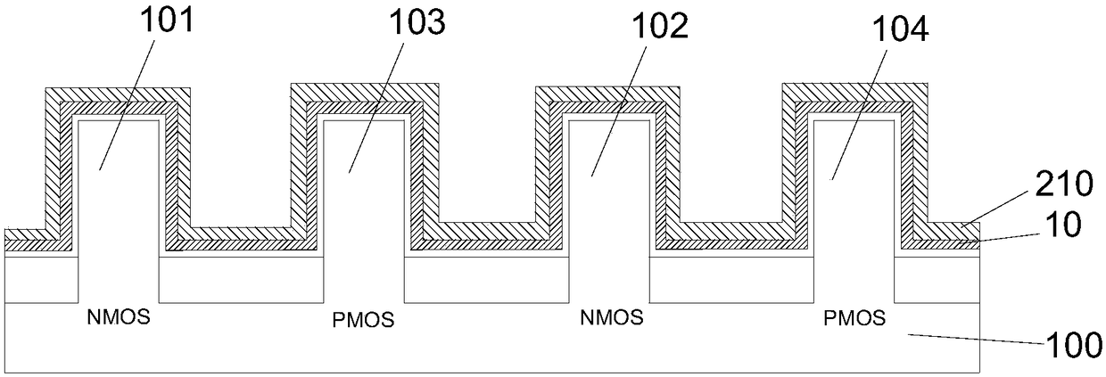
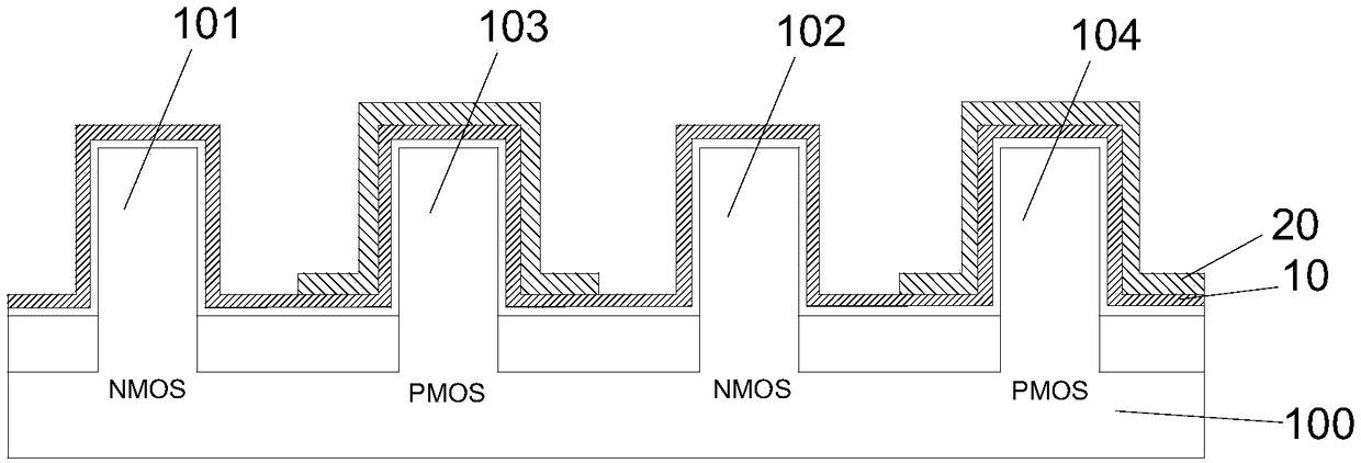
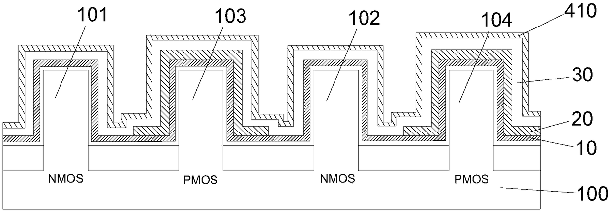
The present invention provides a CMOS device and a method for adjusting the threshold value of a CMOS device. The method includes the following steps that: S1, a substrate is provided, wherein the substrate comprises an NMOS region and a PMOS region, wherein the NMOS region is provided with at least first fin and second fin, and the PMOS region is provided with at least a third fin and a fourth fin; S2, a first barrier layer and a first work function layer are sequentially formed on the substrate, wherein the first barrier layer covers the NMOS region and the PMOS region, the first work function layer is located on a surface of the first barrier layer, wherein the surface of the first barrier layer is not corresponding to the first fin and second fin; S3, a second work function layer and asecond barrier layer are sequentially formed, wherein the second work function layer covers the first barrier layer and the first work function layer, and the second barrier layer covers the second work function layer, positions on the second barrier layer which are corresponding to the first fin and the second fin, have different thicknesses, and positions of the second barrier layer, which arecorresponding to the third fin and the fourth fin, have different thicknesses.

Description

technical field [0001] The invention relates to the technical field of semiconductor integration, in particular to a CMOS device and a method for adjusting the threshold of the CMOS device. Background technique [0002] Existing methods for adjusting the threshold of high-k metal-gate CMOS devices include sequentially depositing a barrier layer and a PMOS work function layer (PMOS WFL) in the process of forming the metal gate stack of NMOS and PMOS, and then removing the PMOS WFL on the NMOS region , and adjust the thickness of the barrier layer on the NMOS region to adjust the NMOS threshold, then adjust the thickness of the PMOSWFL on the PMOS region to adjust the PMOS threshold, and finally deposit the NMOS work function layer (NMOS WFL). [0003] However, in the above-mentioned existing methods, whether it is NMOS or PMOS, the thickness adjustment of the work function threshold of the metal gate is based on the barrier layer and the TiN of the PMOS WFL. x Corrosion of t...

Claims


Application Information

Patent Timeline
IPC IPC(8): H01L21/8238H01L27/092H01L29/10
CPCH01L21/823807H01L21/823821H01L27/0924H01L29/1033
Inventor 殷华湘姚佳欣王文武叶甜春
Owner INST OF MICROELECTRONICS CHINESE ACAD OF SCI
Learn More