Electronic circuit package
A technology of electronic circuits and electronic components, applied in the field of electronic circuit packaging, to achieve the effect of high composite shielding characteristics and high composite shielding effect
- Summary
- Abstract
- Description
- Claims
- Application Information
AI Technical Summary
Problems solved by technology
Method used
Image
Examples
no. 1 Embodiment approach >
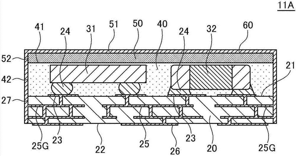
[0075] figure 1 It is a sectional view showing the structure of the electronic circuit package 11A according to the first embodiment of the present invention.
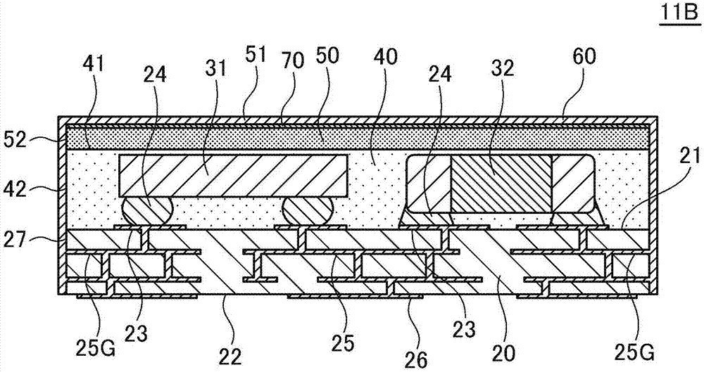
[0076] Such as figure 1 As shown, the electronic circuit package 11A according to this embodiment includes: a substrate 20; a plurality of electronic components 31, 32 mounted on the substrate 20; ; the magnetic film 50 covering the molding resin 40 ; the metal film 60 covering the magnetic film 50 and the molding resin 40 .
[0077] The type of the electronic circuit package 11A according to the present embodiment is not particularly limited, and examples thereof include a high-frequency module for processing high-frequency signals, a power supply module for power control, and a system having a 2.5D structure or a 3D structure. Scale-in-Package (SIP), semiconductor packages for radio communications or digital circuits, etc. exist figure 1 Although only two electronic components 31 and 32 are shown in FIG. 2 , more...
no. 2 Embodiment approach >
[0108] Figure 7 It is a cross-sectional view showing the structure of an electronic circuit package 12A according to the second embodiment of the present invention.
[0109] Such as Figure 7 As shown, the electronic circuit package 12A according to this embodiment is the same as figure 1 The electronic circuit package 11A according to the first embodiment shown is the same. Therefore, the same symbols are attached to the same elements, and overlapping descriptions are omitted.
[0110] In this embodiment, the side surface 27 of the substrate 20 has a stepped shape. Specifically, it has a shape in which the side lower part 27b protrudes more than the side upper part 27a. Therefore, the metal film 60 is not formed on the entire side surface of the substrate 20 , but is provided to cover the side surface 27 a and the step portion 27 c, and the lower side surface 27 b is not covered by the metal film 60 . In the present embodiment, since the power supply pattern 25G is expo...
no. 3 Embodiment approach >
[0117] Figure 11 It is a cross-sectional view showing the structure of an electronic circuit package 13A according to the third embodiment of the present invention.
[0118] Such as Figure 11 The electronic circuit package 13A according to this embodiment shown is the same as that in that the magnetic film 50 covers not only the upper surface 41 but also the side surface 42 of the molding resin 40 . figure 1 The electronic circuit package 11A according to the illustrated first embodiment is different. Since other structures are the same as those of the electronic circuit package 11A according to the first embodiment, the same symbols are assigned to the same elements, and overlapping descriptions are omitted.
[0119] In the present embodiment, since the side surface 42 of the molding resin 40 is completely covered with the magnetic film 50 , there is substantially no portion where the molding resin 40 contacts the metal film 60 . With such a structure, the composite shie...
PUM
 Abstract
Description
Claims
Application Information


