Electronic circuit package

Active Publication Date: 2018-02-01
TDK CORPARATION
View PDF4 Cites 18 Cited by
  • Summary
  • Abstract
  • Description
  • Claims
  • Application Information

AI Technical Summary

Benefits of technology

[0018]As described above, according to the present invention, it is possib

Problems solved by technology

However, this tendency poses a problem of malfunction and radio disturbance due to noise.
The problem of malfunction and radio disturbance is difficult to be solved by conventional noise countermeasure techniques.
However, the configuration described in U.S. Patent Publication No. 2011/0304015 where an adhesive is used to bond the shield case is not only disadvantageous in terms of height reduction, but also makes it harder for the metal film to be connected to a ground pattern on a substrate.
Further, the configuration described in U.S. Patent Publication No. 2013/0307128 where the concave portion formed in the mold resin is filled with

Method used


Image

  • Electronic circuit package
  • Electronic circuit package
  • Electronic circuit package

Examples


first embodiment

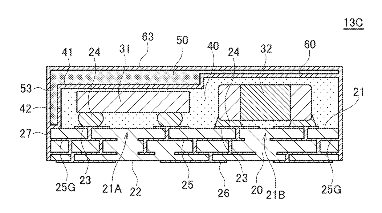
[0039]FIG. 1 is a cross-sectional view illustrating a configuration of an electronic circuit package 11A according to the first embodiment of the present invention.

[0040]As illustrated in FIG. 1, the electronic circuit package 11A according to the present embodiment includes a substrate 20, a plurality of electronic components 31 and 32 mounted on the substrate 20, a mold resin 40 covering a front surface 21 of the substrate 20 so as to embed the electronic components 31 and 32, a magnetic film 50 formed on an upper surface 41 of the mold resin 40, and a metal film 60 covering a side surfaces 42 of the mold resin 40 and an upper surface 51 of the magnetic film 50.

[0041]Although the type of the electronic circuit package 11A according to the present embodiment is not especially limited, examples thereof include a high-frequency module handling a high-frequency signal, a power supply module performing power supply control, an SIP (System-In-Package) having a 2.5D structure or a 3D str...

second embodiment

[0082]FIG. 18 is a cross-sectional view illustrating a configuration of an electronic circuit package 12A according to a second embodiment.

[0083]As illustrated in FIG. 18, the electronic circuit package 12A according to the present embodiment differs from the electronic circuit package 11A illustrated in FIG. 1 in that the lamination order of the magnetic film 50 and the metal film 60 is reversed. That is, the metal film 60 is positioned between the mold resin 40 and the magnetic film 50. Other configurations are the same as those of the electronic circuit package 11A illustrated in FIG. 1. Thus, the same reference numerals are given to the same elements, and overlapping description will be omitted.

[0084]In the present embodiment as well, the region above the electronic component 31 for which noise countermeasures are especially required is covered with the laminated film of the metal film 60 and magnetic film 50 having large thickness, enabling a composite shield characteristic to ...

third embodiment

[0095]FIG. 23 is a cross-sectional view illustrating a configuration of an electronic circuit package 13A according to a third embodiment of the present invention.

[0096]As illustrated in FIG. 23, the electronic circuit package 13A according to the present embodiment differs from the electronic circuit package 12A illustrated in FIG. 18 in that the upper surface of the magnetic film 50 is covered with a metal film 63 different from the metal film 60. Other configurations are the same as those of the electronic circuit package 12A illustrated in FIG. 18. Hence, the same reference numerals are given to the same elements, and overlapping description will be omitted.

[0097]In the present embodiment, the upper surface 41 of the mold resin 40 is covered with a three-layer laminated film of the metal film 60 (first metal film), magnetic film 50, and metal film 63 (second metal film), a thickness of the magnetic film 50 is selectively increased above the electronic component 31 for which nois...


PUM


Abstract

Disclosed herein is an electronic circuit package includes a substrate having a power supply pattern, a first electronic component mounted on a first region of a front surface of the substrate, a mold resin that covers the front surface of the substrate so as to embed the first electronic component therein, and a laminated film covering an upper surface of the mold resin, the laminated film including a magnetic film and a first metal film. The first metal film is connected to the power supply pattern. The magnetic film is selectively thick on the first region.

Description

BACKGROUND OF THE INVENTIONField of the Invention[0001]The present invention relates to an electronic circuit package and, more particularly, to an electronic circuit package provided with a composite shielding function having both an electromagnetic shielding function and a magnetic shielding function.Description of Related Art[0002]In recent years, an electronic device such as a smartphone is equipped with a high-performance radio communication circuit and a high-performance digital chip, and an operating frequency of a semiconductor IC used therein tends to increase. Further, adoption of an SIP (System-In Package) having a 2.5D or 3D structure, in which a plurality of semiconductor ICs are connected by a shortest wiring, is accelerated, and modularization of a power supply system is expected to accelerate. Further, an electronic circuit module having a large number of modulated electronic components (collective term of components, such as passive components (an inductor, a capaci...

Claims


Application Information

Patent Timeline
IPC IPC(8): H01L23/552H01L23/00H01L21/3205H01L25/16H01L21/56H01L23/498H01L23/31
CPCH01L23/552H01L23/49822H01L24/16H01L23/3121H01L23/315H01L25/16H01L24/97H01L23/49838H01L21/561H01L21/32051H01L2224/16227H01L2924/19105H01L2924/3025H01L23/49805H01L23/50H01L24/13H01L2224/131H01L2224/97H01L2924/15192H01L2924/15313H01L2924/1815H01L2924/19041H01L2924/19042H01L2224/81H01L2924/014H01L2924/00014
Inventor KAWABATA, KENICHIHAYAKAWA, TOSHIOOKUBO, TOSHIRO
Owner TDK CORPARATION
Why Eureka
Try Eureka