Electronic circuit package

a technology of electronic components and metal casings, applied in the direction of magnetic bodies, printed circuit non-printed electric components association, and semiconductor/solid-state device details, etc., can solve the problems of difficult to solve malfunction and radio disturbance, difficult to cover the entire structure with metal casings, and difficult to reduce height, so as to facilitate and reliably connect metal films to power supply patterns, suppress fluctuation of characteristics of electronic components, and high composite shielding

Active Publication Date: 2018-02-27
TDK CORPARATION
View PDF14 Cites 4 Cited by
  • Summary
  • Abstract
  • Description
  • Claims
  • Application Information

AI Technical Summary

Benefits of technology

[0006]An object of the present invention is therefore to provide an electronic circuit package capable of realizing both high composite shielding effect and reduction in height and capable of preventing deterioration in magnetic characteristics of a magnetic mold resin due to eddy current.

Problems solved by technology

However, this tendency poses a problem of malfunction and radio disturbance due to noise.
The problem of malfunction and radio disturbance is difficult to be solved by conventional noise countermeasure techniques.
However, in the electronic circuit package disclosed in Japanese Patent Application Laid-Open No. 1984-132196, the covering of the entire structure with the metal casing makes reduction in height difficult.
Further, the metal casing has a large number of holes formed therein and is not connected to a ground pattern of a substrate, so that a sufficient shielding effect cannot be obtained.
In addition, when an eddy current occurs due to incidence of electromagnetic wave noise in the metal casing, the eddy current flows in the magnetic mold resin to deteriorate magnetic characteristics of the magnetic mold resin.

Method used


Image

  • Electronic circuit package
  • Electronic circuit package
  • Electronic circuit package

Examples


first embodiment

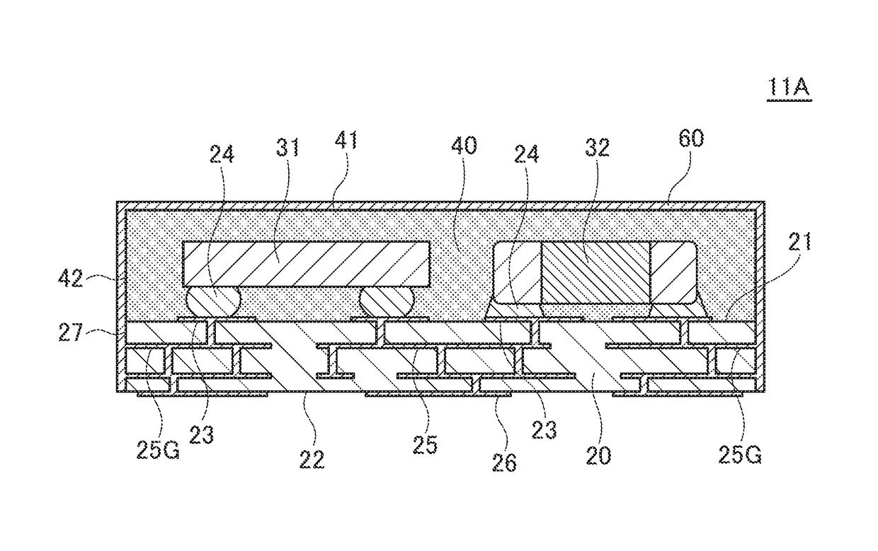
[0031]FIG. 1 is a cross-sectional view illustrating a configuration of an electronic circuit package 11A according to the first embodiment of the present invention.

[0032]As illustrated in FIG. 1, the electronic circuit package 11A according to the present embodiment includes a substrate 20, a plurality of electronic components 31 and 32 mounted on the substrate 20, a magnetic mold resin 40 covering a front surface 21 of the substrate 20 so as to embed the electronic components 31 and 32, and a metal film 60 covering the magnetic mold resin 40.

[0033]Although the type of the electronic circuit package 11A according to the present embodiment is not especially limited, examples thereof include a high-frequency module handling a high-frequency signal, a power supply module performing power supply control, an SIP (System-In-Package) having a 2.5D structure or a 3D structure, and a semiconductor package for radio communication or digital circuit. Although only two electronic components 31 ...

second embodiment

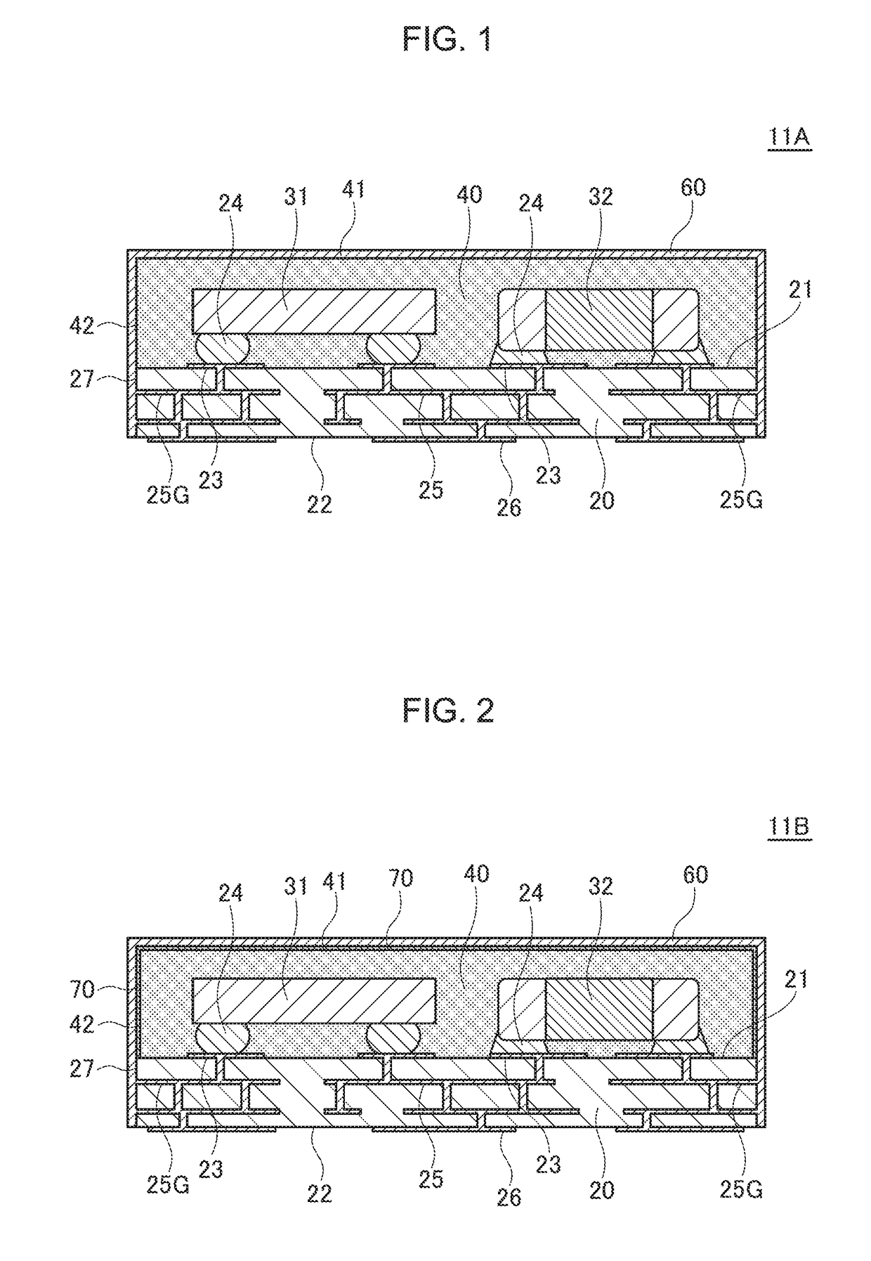
[0059]FIG. 7 is a cross-sectional view illustrating a configuration of an electronic circuit package 12A according to the second embodiment of the present invention.

[0060]As illustrated in FIG. 7, an electronic circuit package 12A according to the present embodiment is the same as the electronic circuit package 11A according to the first embodiment illustrated in FIG. 1 except for shapes of the substrate 20 and metal film 60. Thus, in FIG. 7, the same reference numerals are given to the same elements as in FIG. 1, and repetitive descriptions will be omitted.

[0061]In the present embodiment, the side surface 27 of the substrate 20 is formed stepwise. Specifically, a side surface lower portion 27b protrudes from a side surface upper portion 27a. The metal film 60 is not formed over the entire side surface of the substrate 20 but formed so as to cover the side surface upper portion 27a and a step portion 27c. That is, the side surface lower portion 27b is not covered with the metal film...

third embodiment

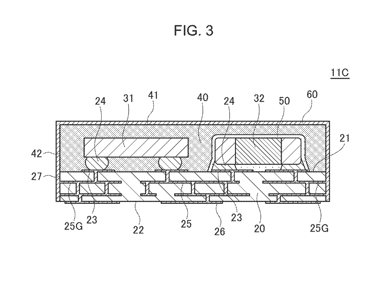
[0068]FIG. 11 is a cross-sectional view illustrating a configuration of an electronic circuit package 13A according to the third embodiment of the present invention.

[0069]As illustrated in FIG. 11, an electronic circuit package 13A according to the present embodiment differs from the electronic circuit package 11A according to the first embodiment illustrated in FIG. 1 in that a planar size of the magnetic mold resin 40 is slightly smaller than a planar size of the substrate 20 and, therefore, an outer peripheral portion of the front surface 21 of the substrate 20 is exposed from the magnetic mold resin 40. Other configurations are the same as those of the electronic circuit package 11A according to the first embodiment. Thus, in FIG. 11, the same reference numerals are given to the same elements as in FIG. 1, and repetitive descriptions will be omitted.

[0070]As exemplified by the electronic circuit package 13A according to the present embodiment, it is not essential in the present ...


PUM

PropertyMeasurementUnit
resistanceaaaaaaaaaa
thicknessaaaaaaaaaa

Abstract

Disclosed herein is an electronic circuit package includes: a substrate having a power supply pattern; an electronic component mounted on a surface of the substrate; a magnetic mold resin formed of a composite magnetic material including a thermosetting resin material and a magnetic filler, the magnetic mold resin covering the surface of the substrate so as to embed therein the electronic component; and a metal film connected to the power supply pattern and covering at least a top surface of the magnetic mold resin. A volume resistance value of the magnetic mold resin is equal to or larger than 1010Ω, and a resistance value at an interface between the top surface of the magnetic mold resin and the metal film is equal to or larger than 106Ω.

Description

BACKGROUND OF THE INVENTIONField of the Invention[0001]The present invention relates to an electronic circuit package and, more particularly, to an electronic circuit package provided with a composite shielding function having both an electromagnetic shielding function and a magnetic shielding function.Description of Related Art[0002]In recent years, an electronic device such as a smartphone is equipped with a high-performance radio communication circuit and a high-performance digital chip, and an operating frequency of a semiconductor IC used therein tends to increase. Further, adoption of an SIP (System-In Package) having a 2.5D or 3D structure, in which a plurality of semiconductor ICs are connected by a shortest wiring, is accelerated, and modularization of a power supply system is expected to accelerate. Further, an electronic circuit module having a large number of modulated electronic components (collective term of components, such as passive components (an inductor, a capaci...

Claims


Application Information

Patent Timeline
Patent Type & Authority Patents(United States)
IPC IPC(8): H05K1/18H01F1/03H05K1/02
CPCH05K1/182H01F1/0306H05K1/0216H01L23/29H01L23/552H01L2924/181H01F1/26H05K1/0298H05K1/181H05K3/284H01L2224/97H01L2924/19105H05K2201/083H05K2203/1316H01L2924/15159H01L2924/15192H01L2924/15313H01L2924/3025H05K9/0024H01L2224/16227H01L25/16H01L2924/19041H01L2924/19042H01L21/565H01L2924/19043H01L23/295H01L2224/131H01L24/13H01L24/16H01L21/561H01L23/3121H01L2924/00012H01L2224/81H01L2924/014H01L2924/00014H01L2224/16225H05K9/003
Inventor KAWABATA, KENICHI
Owner TDK CORPARATION
Why Eureka
Try Eureka