GOA circuit
A circuit and low-voltage technology, applied in the display field, to achieve the effect of solving the Q point potential maintenance and wide pulse GOA signal output
- Summary
- Abstract
- Description
- Claims
- Application Information
AI Technical Summary
Problems solved by technology
Method used
Image
Examples
Embodiment Construction
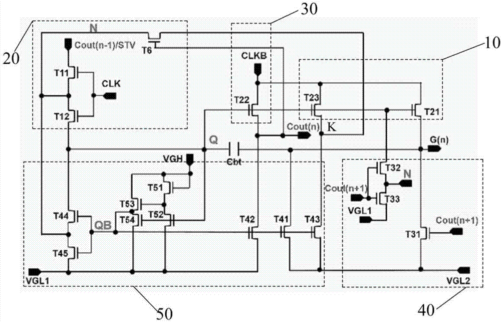
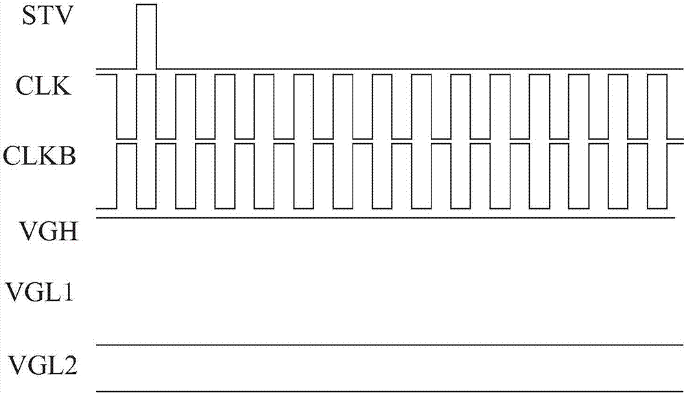
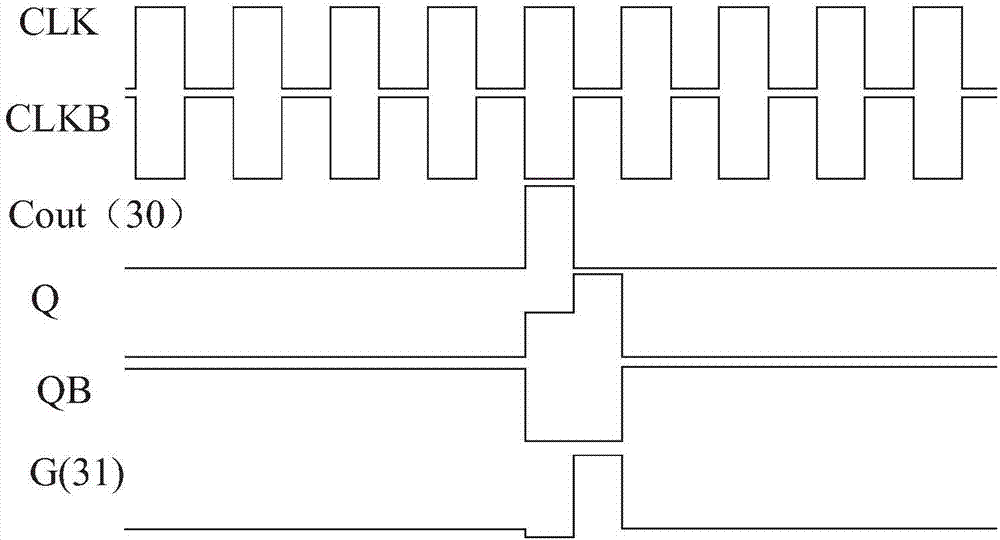
[0040] see figure 1 and figure 2 , this preferred embodiment of the present invention is mainly made of 18 TFTs and a capacitor Cbt, and the connection relationship between the circuits is as follows figure 1 shown. Among them, CLK and CLKB are AC power sources with opposite waveforms, VGH, VGL1 and VGL2 are DC power sources, and STV is a start pulse (start pulse) trigger signal, which is required for starting the first-stage GOA unit. The specific waveform and voltage relationship of each signal in the GOA circuit can be shown in the table below. Nodes N, Q, QB, Cout(n-1), Cout(n), Cout(n+1), G(n), etc. are important nodes in the circuit.
[0041]
[0042] Other parameters of the panel applying this preferred embodiment can be set as follows: for FHD (full high definition) resolution, the number of row scanning lines is 1080, the number of clock signals (CK number) is 2 (CLK and CLKB), and the clock cycle ( CK period) is 336 milliseconds, the duty cycle (Duty cycle) i...
PUM
 Abstract
Description
Claims
Application Information


