Goa circuit
a goa circuit and circuit technology, applied in the field of goa circuits, can solve problems such as goa circuit failure, and achieve the effect of wide pulse goa signal outpu
- Summary
- Abstract
- Description
- Claims
- Application Information
AI Technical Summary
Benefits of technology
Problems solved by technology
Method used
Image
Examples
Embodiment Construction
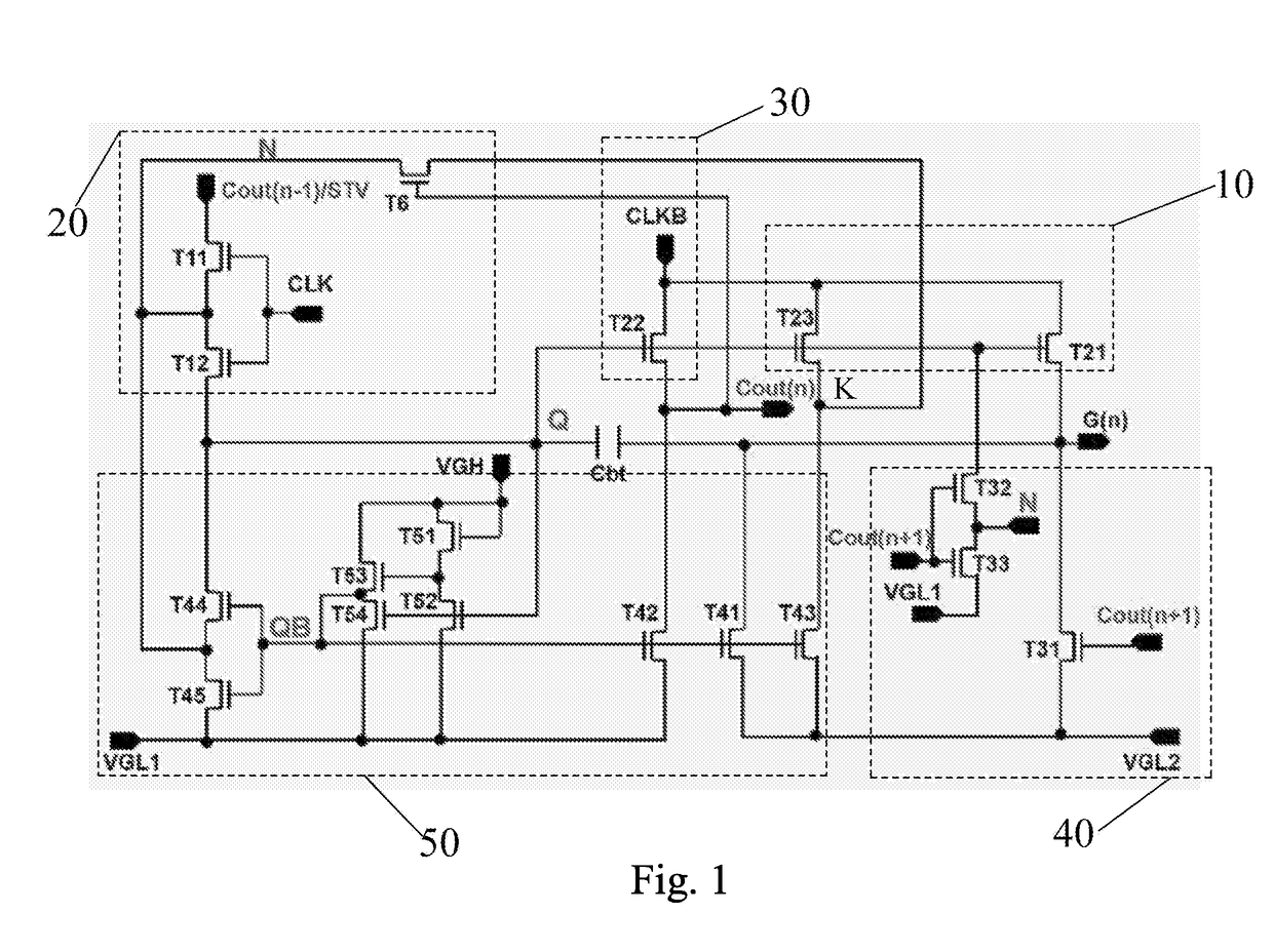
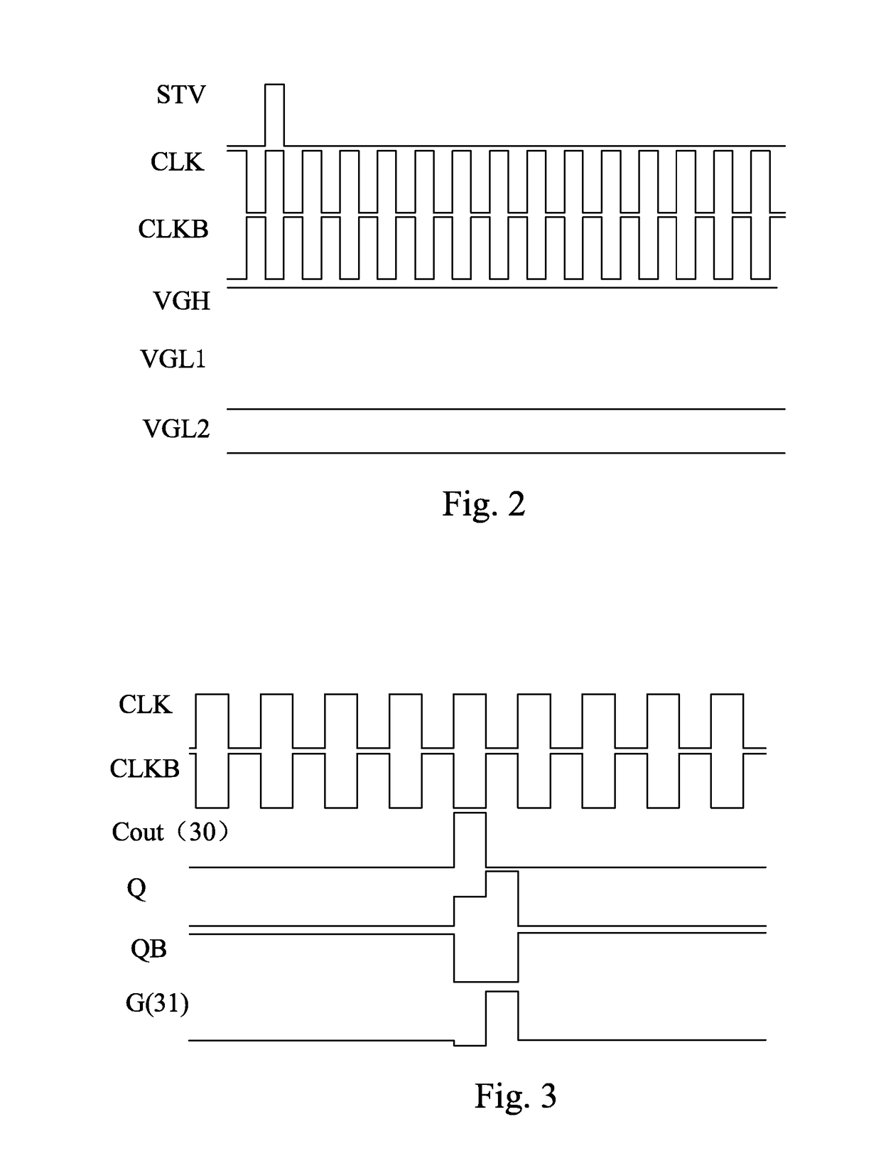
[0051]Referring to FIG. 1 and FIG. 2, the preferred embodiment of the present invention comprises 18 TFTs and a capacitor Cbt. The interconnection of the element is as shown in FIG. 1. CLK and CLKB are alternating current power source with opposite phases, VGH, VGL1 and VGL2 are DC power source, and STV is the start pulse trigger signal, which is for activating the first GOA unit in the cascade. The relation between specific waveform and voltage of each signal in the GOA circuit is shown in Table 1. The nodes N, Q, QB, Count(n−1), Count(n), Count(n+1), and G(n) are important nodes in the circuit.
voltageGOA signalMin (volts)Max (volts)STV−10+30CLK−10+30CLKB−10+30VGH+30VGL1−10VGL2−6
[0052]The other panel parameters applied to the preferred embodiment can be set as follows: for FHD, the number of scan lines is 1080, the number of clock signals (CK number) is 2, i.e., CLK and CLKB, the clock period is 336 ms, duty cycle is 50%, and STV width is 168 ms.
[0053]The n-th GOA unit of the prese...
PUM
 Abstract
Description
Claims
Application Information


