Display panel and display device

A display panel and substrate technology, applied to static indicators, instruments, etc., can solve the problems of reducing the drift degree of control transistors, display unevenness, etc.

Active Publication Date: 2017-12-15
WUHAN TIANMA MICRO ELECTRONICS CO LTD
View PDF8 Cites 14 Cited by
  • Summary
  • Abstract
  • Description
  • Claims
  • Application Information

AI Technical Summary

Problems solved by technology

[0004] In view of this, the present invention provides a display panel and a display device. At least one hollow structure is provided on the continuous gate structure of the control transistor electrically connected to the gate of the driving module, so that a plurality of sub-transistors are formed in one control transistor, The voltage between the source and the drain of each sub-tr

Method used


Image

  • Display panel and display device
  • Display panel and display device
  • Display panel and display device

Examples


Embodiment Construction

[0026] The present invention will be further described in detail below in conjunction with the accompanying drawings and embodiments. It should be understood that the specific embodiments described here are only used to explain the present invention, but not to limit the present invention. In addition, it should be noted that, for the convenience of description, only some structures related to the present invention are shown in the drawings but not all structures. Throughout this specification, the same or similar reference numerals represent the same or similar structures, elements or processes. It should be noted that, in the case of no conflict, the embodiments in the present application and the features in the embodiments can be combined with each other.

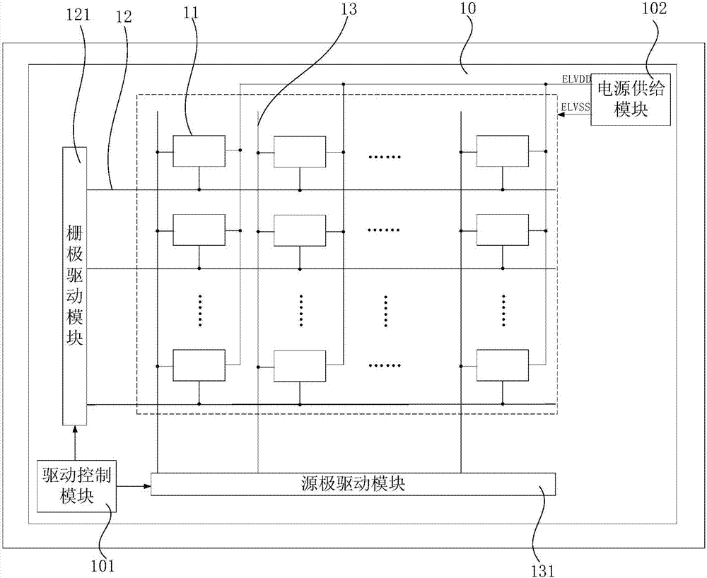
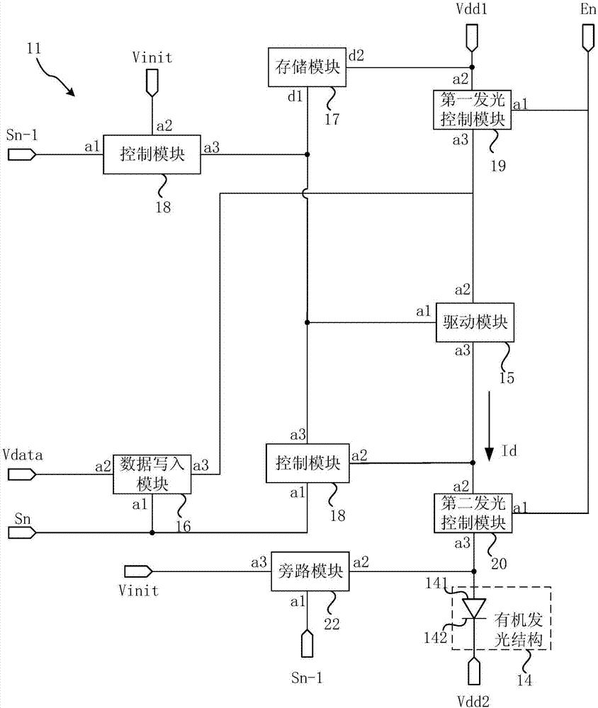
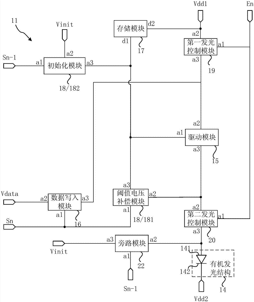
[0027] An embodiment of the present invention provides a display panel, including a substrate and a plurality of pixel circuits on the substrate, each pixel circuit includes a driving module, a data writing module, a st...


PUM

PropertyMeasurementUnit
Widthaaaaaaaaaa
Lengthaaaaaaaaaa

Abstract

The present invention discloses a display panel and a display device. Each pixel circuit in a display panel comprises a driving module, an organic luminescence structure, data write-in module, a storage module and at least one control module, wherein the data write-in module writes data signals in the control end of the driving module; the storage module is electrically connected with the control end of the driving module to maintain the voltage of the driving module at the control end of a luminescence phase; the control module is electrically connected with the control end of the driving module, signals are written into the control end of the driving module prior to the luminescence phase; and the continuous grid structure of a control transistor in the control module comprises at least one hollow structure, the vertical projection of the hollow structure on the substrate covers part of vertical projection of the continuous grid structure on the substrate, and the projection area of the hollow area on the substrate is larger than the projection area of the continuous grid structure corresponding to the hollow structure on the substrate. The problem is improved that the display of the display device is not uniform.

Description

technical field [0001] Embodiments of the present invention relate to the field of display technology, and in particular, to a display panel and a display device. Background technique [0002] An organic light emitting display device generally includes several pixels, and each pixel includes a pixel driving circuit. The pixel circuit with the simplest structure used in the prior art is a 2T1C structure, that is, the pixel circuit includes two transistors and a storage capacitor, one of which is a switching transistor, and the other transistor is a drive transistor that drives the organic light-emitting structure in the pixel to emit light The pixel circuit may further include a control transistor electrically connected to the gate of the drive transistor, and the control transistor may write a signal into the gate of the drive transistor before the light-emitting phase. The control transistors correspond to a transfer characteristic curve. The transfer characteristic curve ...

Claims


Application Information

Patent Timeline
IPC IPC(8): G09G3/3208
CPCG09G3/3208G09G2300/0426G09G2300/0819G09G2300/0842G09G2300/0861G09G2310/0251G09G2310/0262G09G2320/043G09G3/3233G09G2320/0214
Inventor 席克瑞崔婷婷林柏全欧阳珺婷周瑞渊
Owner WUHAN TIANMA MICRO ELECTRONICS CO LTD
Why Eureka
Try Eureka