Machining method of digital-analog printed circuit board

A technology of printed circuit boards and processing methods, which is applied in the directions of printed circuits, printed circuit manufacturing, multilayer circuit manufacturing, etc., and can solve problems such as unrealizable

Active Publication Date: 2017-12-15
珠海杰赛科技有限公司 +1
View PDF7 Cites 0 Cited by
  • Summary
  • Abstract
  • Description
  • Claims
  • Application Information

AI Technical Summary

Problems solved by technology

[0003] The purpose of the present invention is to provide a processing method for digital-analog printed circuit boards, which solves the problem that if the digital-analog PCB product produced has various structures such as cross blind holes, partial embedding and blind grooves, the existing conventional process unachievable problem

Method used


Image

  • Machining method of digital-analog printed circuit board

Examples


Embodiment Construction

[0023] Specific embodiments of the present invention will be described in detail below. It should be understood that the specific embodiments described here are only used to illustrate and explain the present invention, and are not intended to limit the present invention.

[0024] Neither the endpoints nor any values ​​of the ranges disclosed herein are limited to such precise ranges or values, and these ranges or values ​​are understood to include values ​​approaching these ranges or values. For numerical ranges, between the endpoints of each range, between the endpoints of each range and individual point values, and between individual point values ​​can be combined with each other to obtain one or more new numerical ranges, these values Ranges should be considered as specifically disclosed herein.

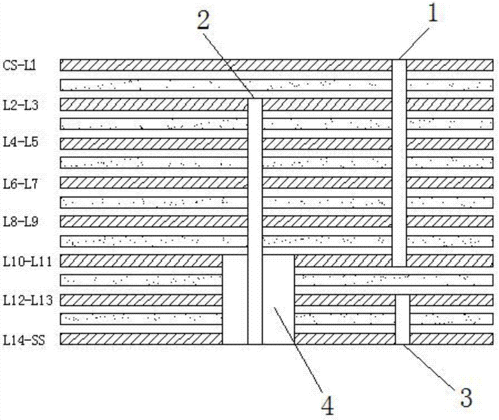
[0025] The invention provides a processing method of a digital-to-analog printed circuit board, the processing method comprising:

[0026] 1) Carry out material cutting, graphi...


PUM


Abstract

The invention discloses a machining method of a digital-analog printed circuit board. The machining method comprises the steps that 1, cutting, pattern transferring, deep milling control and brownification are performed on digital layer L12-L13 core plates; 2, cutting and hole milling are performed on PP materials between the layers L11 and L12; 3, laminating, hole drilling and hole forming are performed on the digital layer L2-SS core plates to form second blind holes, and then pattern transferring, anti-etching layer plating and brownification are performed; 4, laminating and blind groove milling are performed on digital layer CS-SS core plates to obtain column bosses, blind hole machining is performed on the bottoms of the column bosses, and first blind holes are formed; 5, laminating, hole drilling and form forming are performed on radio frequency layer L12-SS core plates to obtain third blind holes, and then pattern transferring, hole milling and brownification are performed; 6, wedge press-fitting is performed on the digital layer CS-L11 and radio frequency layer L12-SS. The problem that when produced digital-analog PCB products are of crossed blind holes, local inserts, blind grooves and other structures, the products cannot be obtained according to an existing conventional technology is solved.

Description

technical field [0001] The invention relates to the field of digital-analog printed circuit boards, in particular to a processing method for digital-analog printed circuit boards. Background technique [0002] When a digital-analog PCB product has the characteristics of cross-blind hole, partial embedding and blind slot structure, the overall realization process of processing. Ordinary digital-to-analog printed circuit boards usually do not integrate multiple structures, the product technology is relatively single, and the implementation process is relatively simple. Now there are relatively mature processes in the entire PCB manufacturing industry to follow. However, if the digital-analog PCB products produced have various structures such as cross blind holes, partial embedding and blind slots, it cannot be realized according to the existing conventional technology. There is no process to follow for PCB products with this structure in the current PCB manufacturing industry...

Claims


Application Information

Patent Timeline
Patent Type & Authority Applications(China)
IPC IPC(8): H05K3/46
CPCH05K3/4688H05K2203/068
Inventor 唐有军李超谋关志锋
Owner 珠海杰赛科技有限公司
Why Eureka
Try Eureka