
Array substrate and manufacturing method and display device

A technology of an array substrate and a manufacturing method, applied in the field of liquid crystal panels, can solve the problems affecting the appearance of the display and the like

Inactive Publication Date: 2017-12-29
TCL CHINA STAR OPTOELECTRONICS TECH CO LTD
View PDF5 Cites 19 Cited by
  • Summary
  • Abstract
  • Description
  • Claims
  • Application Information

AI Technical Summary

Problems solved by technology

[0003] In the production process of the liquid crystal display, due to the needs of the liquid crystal drive, it is necessary to reserve a bonding (bonding) area for the driving circuit. The OLB (external pin) for contacting the COF substrate with the data line and the scanning line is set in the bonding area. terminal), the traditional method is to make the TFT (thin film transistor) substrate with lines slightly larger (usually greater than 1mm) than the upper CF (color filter) substrate, and set the binding area at this position, In order to reserve the binding position of the drive line, but this requires an outer frame to cover the binding area so as not to affect the display appearance

Method used


Image

  • Array substrate and manufacturing method and display device
  • Array substrate and manufacturing method and display device
  • Array substrate and manufacturing method and display device

Examples


Embodiment Construction

[0025] The present invention will be described in further detail below in conjunction with the accompanying drawings and embodiments.

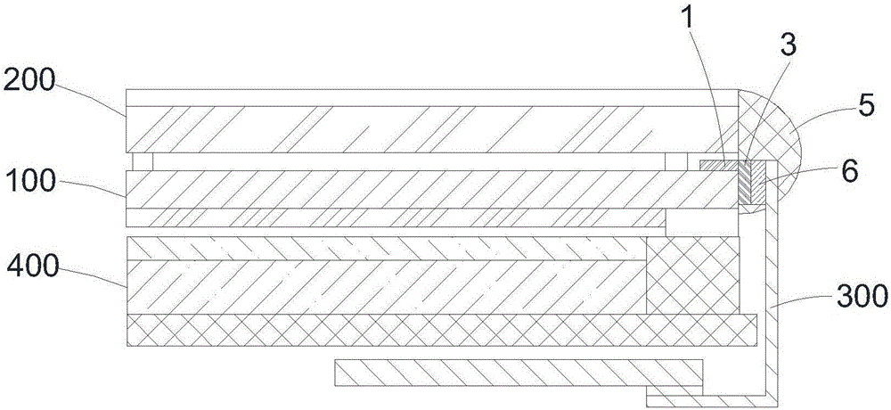
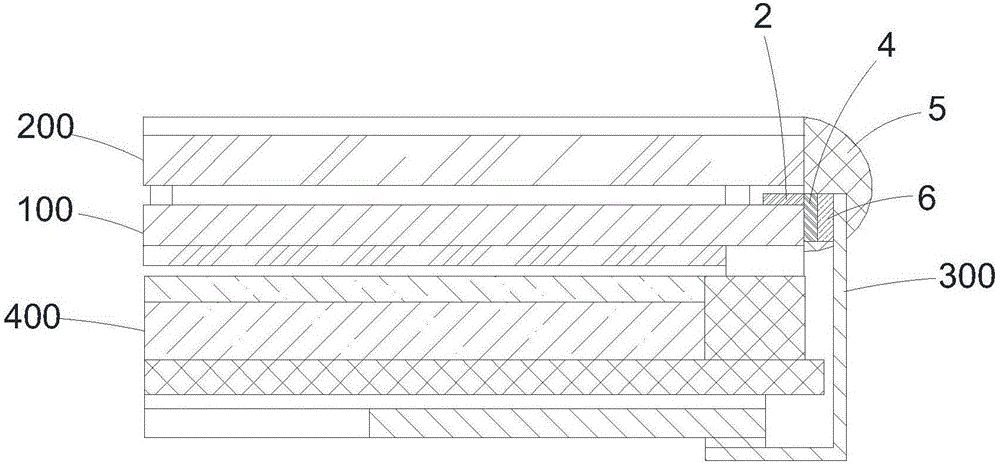
[0026] Figure 1-Figure 5 In order to clearly understand the present invention, the structure of the array substrate is omitted, simplified and exaggerated, but it is worth noting that the internal structure of the array substrate is not changed in the present invention, only the setting position of the binding region and The setting position of the external pin end; the schematic drawings and embodiments shown in conjunction with the accompanying drawings are to explain the principle of the present invention and its practical application, so that other skilled persons in the art can understand various embodiments of the present invention with various modifications as are suited to the particular intended application.

[0027] Such as figure 1 and figure 2 As shown, the array substrate 100 of the present invention includes a plurality of s...


PUM


Abstract

The invention provides an array substrate. The array substrate comprises a scanning line, a data line, a first external pin end and a second external pin end, wherein the first external pin end and the second external pin end make contact with the scanning line and the data line respectively, the first external pin end is arranged on the side edge, vertical to the scanning line, of the array substrate, and the second external pin end is arranged on the side edge, vertical to the data line, of the array substrate. The invention provides a manufacturing method of the array substrate and a display device. Compared with the prior art, a binding region on the array substrate is arranged on the side edge vertical to the data line and the scanning line, the step that a binding region needs to be arranged in a non-display region of the array substrate is omitted, the array substrate and a color filter substrate are cut into identical sizes, and then an unframed display device is obtained.

Description

technical field [0001] The invention relates to a liquid crystal panel technology, in particular to an array substrate, a manufacturing method thereof, and a display device. Background technique [0002] In recent years, the liquid crystal display industry has continued to develop, and the appearance of the panel has gradually become narrower. For example, the narrow bezel TV narrows the non-display area at the edge, and the bezel adopts a more concise and detailed shape to make the product more beautiful. In addition to narrow bezels, the concept of "borderless" panels is even proposed, that is, the outer frame that blocks the non-display area of ​​the panel is removed to achieve a borderless display. [0003] In the production process of the liquid crystal display, due to the needs of the liquid crystal drive, it is necessary to reserve a bonding (bonding) area for the driving circuit. The OLB (external pin) for contacting the COF substrate with the data line and the scann...

Claims


Application Information

Patent Timeline
Patent Type & Authority Applications(China)
IPC IPC(8): G02F1/1345G02F1/1333G02F1/1335
CPCG02F1/13452G02F1/1333G02F1/133351G02F1/133512
Inventor 周凯锋张伟基
Owner TCL CHINA STAR OPTOELECTRONICS TECH CO LTD
Learn More