Array substrate and display panel

一种阵列基板、薄膜晶体管的技术,应用在静态指示器、光学、仪器等方向,能够解决显示不均、影响像素单元像素电压等问题,达到显示画面质量高、显示效果均匀的效果

Active Publication Date: 2018-02-16
WUHAN CHINA STAR OPTOELECTRONICS TECH CO LTD
View PDF6 Cites 3 Cited by
  • Summary
  • Abstract
  • Description
  • Claims
  • Application Information

AI Technical Summary

Problems solved by technology

Due to the resistance-capacitance delay on the scan line, the signal at the start and end of the scan line will be different, which directly affects the pixel voltage of the pixel unit at the start and end of the scan line
The larger the panel, the longer the scan line, the more serious the resistance-capacitance delay, and the more obvious the pixel voltage difference between the pixel units at both ends of the scan line, resulting in the brightness on both sides of the panel being greater than the brightness in the middle, resulting in uneven display

Method used


Image

  • Array substrate and display panel
  • Array substrate and display panel
  • Array substrate and display panel

Examples


Embodiment Construction

[0018] The following will clearly and completely describe the technical solutions in the embodiments of the present invention with reference to the drawings in the embodiments of the present invention.

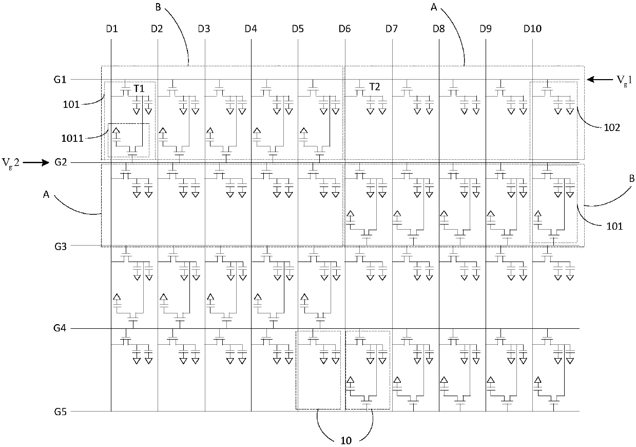
[0019] The present invention provides the array substrate of the first embodiment. See figure 1 , the array substrate disclosed in this embodiment includes:

[0020] A plurality of scanning lines Gn, this embodiment takes the scanning lines G1 to G5 as an example for illustration;

[0021] A plurality of data lines Dn, this embodiment is described by taking the data lines D1 to D10 as an example, and are arranged to intersect with a plurality of scanning lines Gn to form a plurality of pixel units 10;

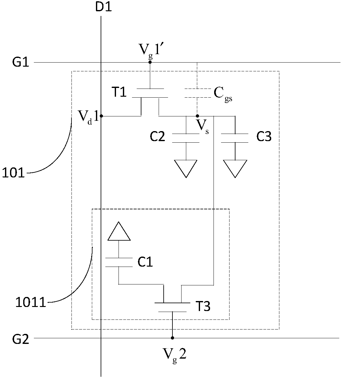
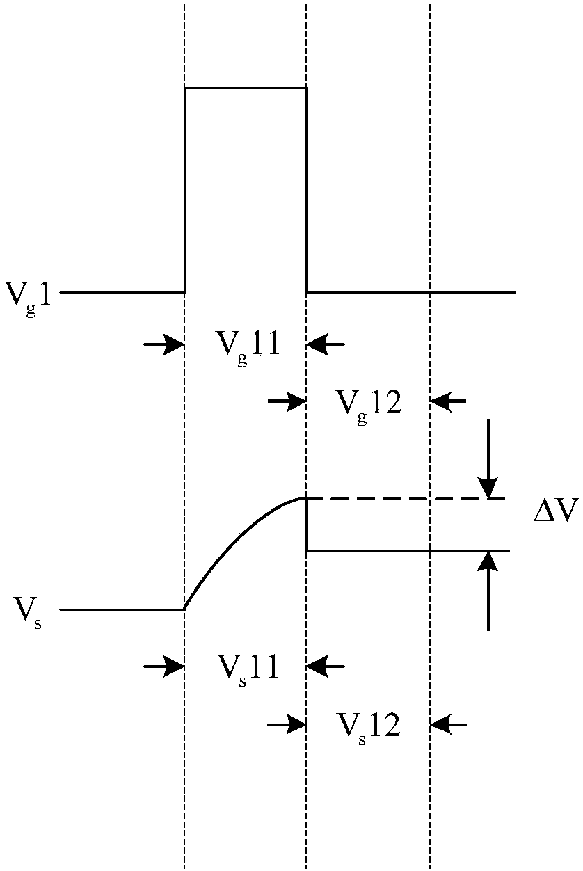
[0022] Wherein, the plurality of pixel units 10 are divided into a first area A and a second area B along the direction of the scanning line Gn, the first area A is close to the scanning signal input end, and the second area B is far away from the scanning signal input end. ...


PUM


Abstract

The invention discloses an array substrate and a display panel. The array substrate comprises multiple scanning lines and data lines arranged in an intersecting mode to form multiple pixel units; themultiple pixel units are divided into a first region and a second region along the scanning lines, the first region is close to the scanning signal input end, and each pixel unit in the second regioncomprises a first thin film transistor and a control unit connected with the first thin film transistor, wherein the control unit is used for reducing pixel voltage of the pixel unit where the first thin film transistor is located. The array substrate is capable of improving the uniformity effect of the display panel and promoting panel display quality.

Description

technical field [0001] The present invention relates to the field of display technology, in particular to an array substrate and a display panel. Background technique [0002] The thin film transistors used in liquid crystal displays usually include amorphous silicon thin film transistors and polycrystalline silicon thin film transistors. Among them, amorphous silicon thin film transistors have low mobility and serious photosensitive degradation as the use time increases; while LTPS (LowTemperaturePoly-silicon , low-temperature polysilicon technology) has high mobility and stability. [0003] The inventors of the present application have found in the long-term research and development that when designing the GOA (Gate Driver on Array, array substrate gate drive) of the LTPS panel, the interlaced scanning mode of unidirectional driving is usually used, that is, GOA is provided on the left and right sides, Interval opening is performed according to the timing of scan line sca...

Claims


Application Information

Patent Timeline
Patent Type & Authority Applications(China)
IPC IPC(8): G02F1/1362
CPCG02F1/1362G02F1/136286G09G2300/0852G09G2300/0426G02F1/13624G09G3/3659G09G3/3648G09G2320/0233G02F1/1368G09G3/3677G09G2300/0819H01L27/124H01L27/1255
Inventor 张婷婷王聪
Owner WUHAN CHINA STAR OPTOELECTRONICS TECH CO LTD
Why Eureka
Try Eureka