Pixel driving circuit and method, and display device

A pixel driving circuit and pixel technology, applied in static indicators, instruments, etc., can solve the problems of low light transmittance, white screen, white display screen, etc., to improve scanning speed, avoid display screen white, Solve the effect of whitening the display screen

Active Publication Date: 2018-11-02
TCL CHINA STAR OPTOELECTRONICS TECH CO LTD
View PDF9 Cites 2 Cited by
  • Summary
  • Abstract
  • Description
  • Claims
  • Application Information

AI Technical Summary

Problems solved by technology

However, large-sized liquid crystal display devices have the problem of visual whitening in the state of large viewing angles, which is caused by the inconsistency between the light transmittance in the state of large viewing angles and the light transmittance in the state of front view, specifically, at low In the case of grayscale, the light transmittance seen by the human eye under the state of large viewing angle is higher than that seen by the human eye under the state of front view. The transmittance is lower than the light transmittance seen by the human eye in the state of frontal vision, and the human eye is more sensitive to low-gray-scale light, so the display screen seen in the state of large viewing angle will be whiter than the picture seen in the state of frontal view. How to solve the problem of whitening of the display screen under large viewing angles has become the focus of research in the field of display devices

Method used


Image

  • Pixel driving circuit and method, and display device
  • Pixel driving circuit and method, and display device
  • Pixel driving circuit and method, and display device

Examples


Embodiment Construction

[0031] In order to further illustrate the technical means adopted by the present invention and its effects, the following describes in detail in conjunction with preferred embodiments of the present invention and accompanying drawings.

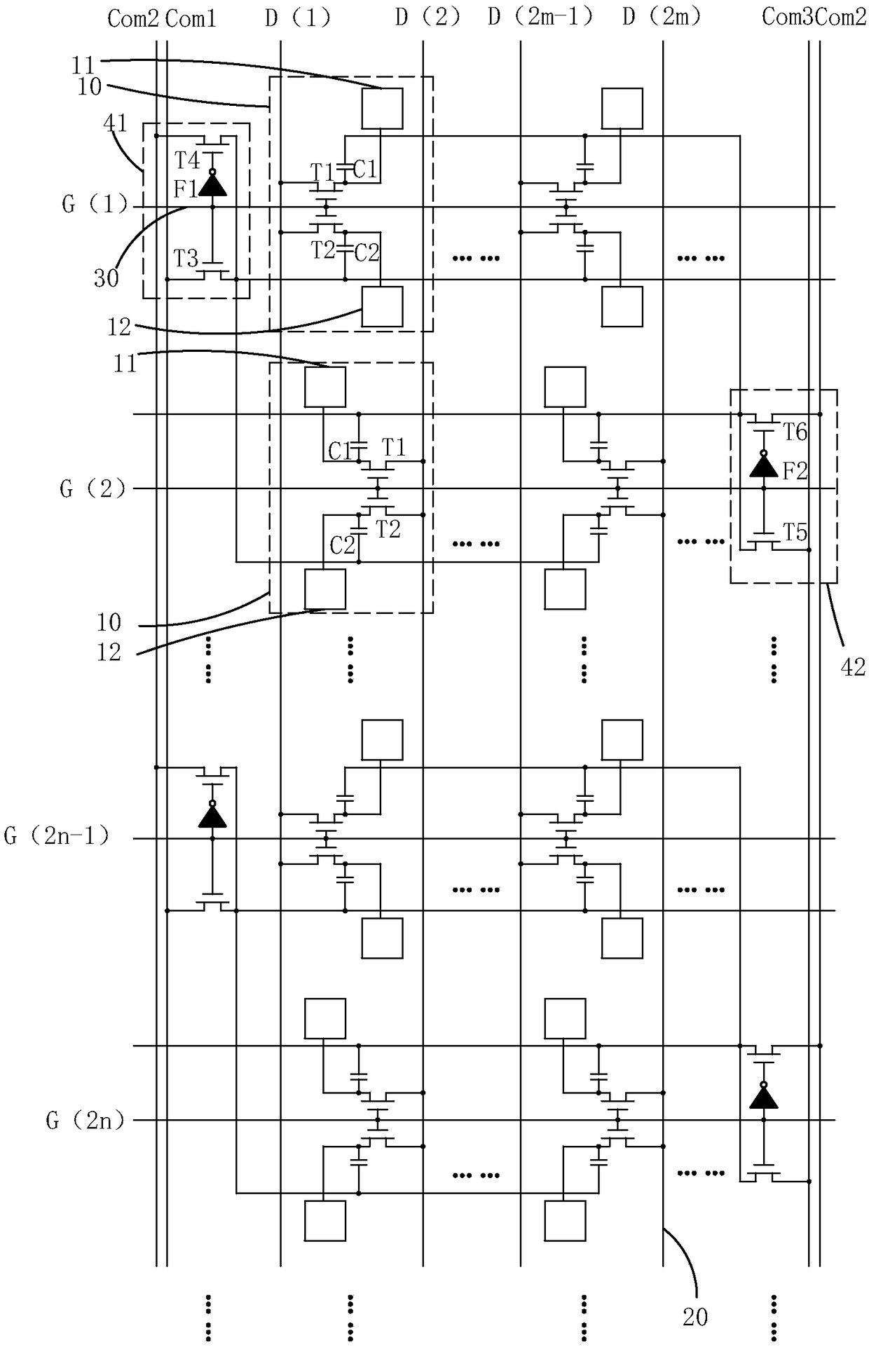
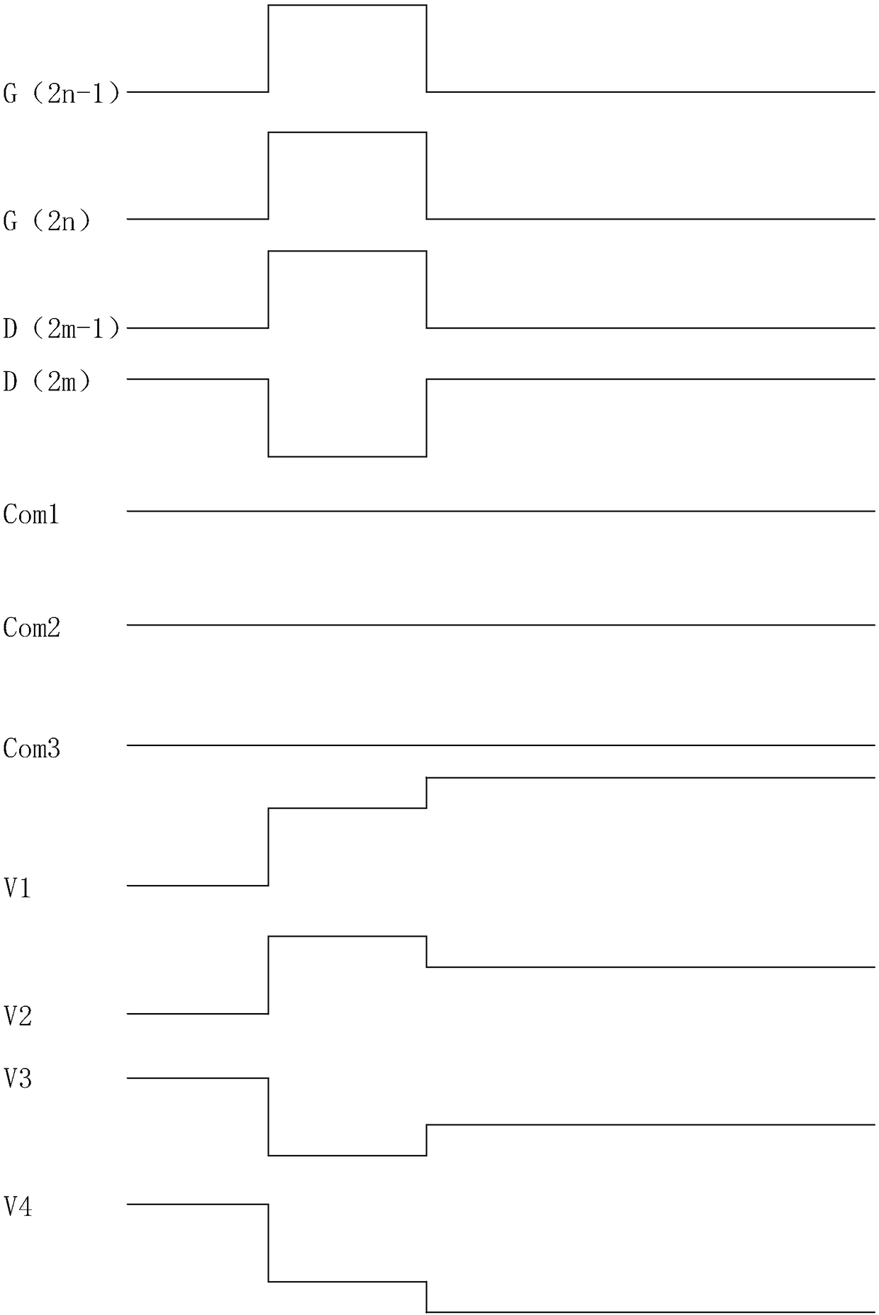
[0032] see figure 1 and figure 2 , the present invention provides a pixel driving circuit, including a plurality of sub-pixels 10 arranged in an array, a plurality of data lines 20 (D(1), D(2)...D(2m-1), D(2m)... ) and scanning lines 30 (G(1), G(2)...G(2n-1), G(2n)...), a plurality of first voltage regulation modules 41 and a plurality of second voltage regulation modules 42.

[0033] Each scanning line 30 is correspondingly connected to a row of sub-pixels 10; a column of sub-pixels 10 is correspondingly connected to two data lines 20, and the odd-numbered row of sub-pixels 10 in the column of sub-pixels 10 is connected to one of the corresponding two data lines 20. The sub-pixels 10 in even rows in 10 are connected to the other one of the c...


PUM


Abstract

The invention provides a pixel driving circuit and method, and a display device. The pixel driving circuit comprises multiple sub pixels arranged in an array mode, multiple data lines and scanning lines and multiple first and second voltage adjusting modules, in the driving process, sub pixels in a (2n 1)th row and sub pixels in a 2nth row are scanned, a first voltage regulating module is used forrespectively inputting a first common voltage and a second common voltage to a second end of a second capacitor of the connected sub pixels when a first film transistor of the connected sub pixels isturned on and off, and a second voltage regulating module is used for respectively inputting a third common voltage and the second common voltage to a second end of a first capacitor of the connectedsub pixels when the first film transistor of the connected sub pixels is turned on and off. The scanning speed of the pixel driving circuit is greatly improved, a first pixel electrode and a second pixel electrode in the same sub pixel can be inputted with different voltages, and a problem that a display frame is whitened existing in the display device in a large viewing angle state is effectively solved.

Description

technical field [0001] The invention relates to the technical field of liquid crystal display, in particular to a pixel driving circuit, a pixel driving method and a display device. Background technique [0002] A liquid crystal display device (Liquid Crystal Display, LCD) is one of the most widely used flat panel displays at present, and a liquid crystal panel is a core component of the liquid crystal display device. A liquid crystal panel usually consists of a color filter substrate (Color Filter Substrate, CF Substrate), a thin film transistor array substrate (Thin FilmTransistor Array Substrate, TFT Array Substrate), and a liquid crystal layer (Liquid Crystal Layer) arranged between the two substrates. constituted. Generally, pixel electrodes and common electrodes are respectively arranged on the array substrate and the color filter substrate. When a voltage is applied to the pixel electrode and the common electrode, an electric field will be generated in the liquid cr...

Claims


Application Information

Patent Timeline
Patent Type & Authority Applications(China)
IPC IPC(8): G09G3/36
CPCG09G3/3607G09G3/3677G09G3/3688G09G3/3696
Inventor 谢剑星
Owner TCL CHINA STAR OPTOELECTRONICS TECH CO LTD
Why Eureka
Try Eureka