Silicon chip surface defect detector capable of classifying defects and defect classifying method

A technology for defect classification and silicon wafer surface, which is applied in the direction of optical defect/defect, instrument, scattering characteristic measurement, etc. It can solve the problems of defect detection function, unable to analyze the spatial distribution of scattered light, and unable to classify defects, etc., to reduce the focus spot , Measuring the effect of signal-to-noise ratio enhancement and fast speed

Inactive Publication Date: 2010-03-17
SHANGHAI INST OF OPTICS & FINE MECHANICS CHINESE ACAD OF SCI
View PDF1 Cites 30 Cited by
  • Summary
  • Abstract
  • Description
  • Claims
  • Application Information

AI Technical Summary

Problems solved by technology

The plano-convex lens focuses all the scattered light within the collection angle to the photodetector, and cannot analyze the spatial distribution of the scattered light
[0005] Existing patents only have the function of detecting defects, but cannot classify defects

Method used


Image

  • Silicon chip surface defect detector capable of classifying defects and defect classifying method
  • Silicon chip surface defect detector capable of classifying defects and defect classifying method

Examples


Embodiment Construction

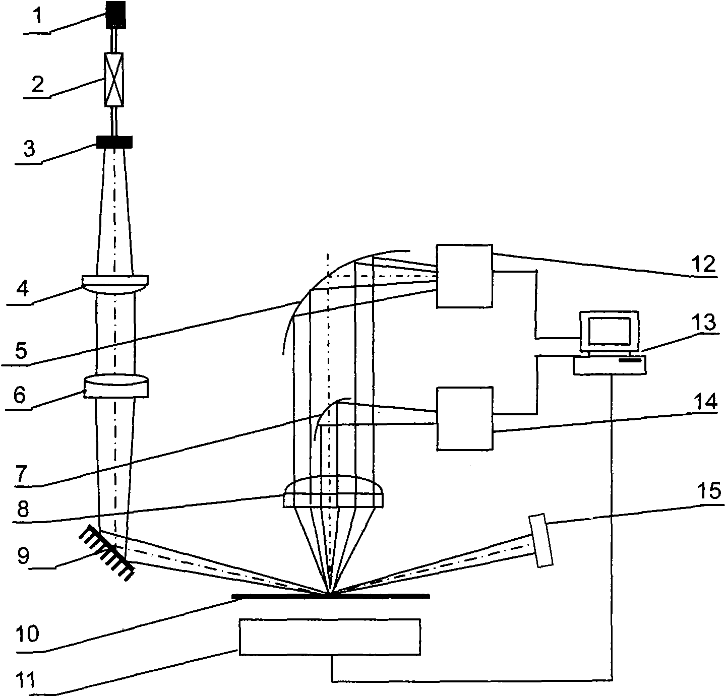
[0031] see first figure 1 . figure 1 It is a schematic diagram of the principle of the silicon wafer surface defect detection system with defect classification capability of the present invention, and is also a structural schematic diagram of the best embodiment of the present invention. It can be seen from the figure that the silicon wafer surface defect detector with defect classification capability of the present invention comprises: in the direction of the light beam emitted by the laser light source assembly 1, there are sequentially an isolator 2, a biconcave lens 3 and a first plano-convex lens 4 Composed of a beam expander system, a double cemented focusing lens 6 and a plane mirror 9; the silicon wafer 10 to be measured is located on a silicon wafer workbench 11 capable of simultaneous rotation and off-axis translation; the light beam is turned by the plane mirror 9 Oblique focusing is incident on the surface of the silicon wafer 10 to be measured, and an optical t...


PUM

PropertyMeasurementUnit
diameteraaaaaaaaaa
poweraaaaaaaaaa
diameteraaaaaaaaaa

Abstract

The invention relates to a silicon chip surface defect detector capable of classifying defects and a defect classifying method. The flat surface of the silicon chip to be detected on a highly reliablesilicon chip working platform is irradiated by a laser from an inclination direction. Circular narrow channel collection and annular narrow channel collection are carried out on scattered lights produced by the silicon chip surface defect by two paraboloidal mirrors with different calibers in a direction near the silicon chip face normal and parallel with silicon chip face. Two photoelectric detectors detect intensities of the collected electrooptical signals in two channels respectively and then take a ratio of two intensities, then compare the ratio with a given threshold value, and at lastthe silicon chip surface defects can be classified. The defect detector has the advantages of simple structure, high sensitivity, fast detecting speed, capability of classifying the defects on the silicon chip surface, etc.

Description

technical field [0001] The invention relates to silicon wafers, in particular to a silicon wafer surface defect detector with defect classification capability and a defect classification method. Background technique [0002] The silicon wafer surface defect detector is an indispensable supporting online inspection equipment for the chip production line. Every process in the production of integrated circuit chips may introduce defects and contamination mechanically or artificially. In the production process of large scale integrated circuits (hereinafter abbreviated as VLSI), detection and classification of defects are important issues related to production yield. [0003] Modern large-scale integrated circuits require the resolution of circuit chip defect detection equipment to be 1 / 3 of its minimum line width. With such a high resolution, it is difficult for traditional detection technology to meet the requirements. With the continuous improvement of VLSI integration and ...

Claims


Application Information

Patent Timeline
Patent Type & Authority Applications(China)
IPC IPC(8): G01N21/88G01N21/49G02B1/00G02B17/08
Inventor 陈建芳程兆谷王毅强许永锋敖计祥黄惠杰
Owner SHANGHAI INST OF OPTICS & FINE MECHANICS CHINESE ACAD OF SCI
Why Eureka
Try Eureka