Electronic device system
An electronic equipment system and circuit technology, applied in the direction of digital output to display equipment, electrical components, electrical digital data processing, etc., can solve problems such as transmission obstacles of display driver data
- Summary
- Abstract
- Description
- Claims
- Application Information
AI Technical Summary
Problems solved by technology
Method used
Image

Examples
Embodiment approach 1
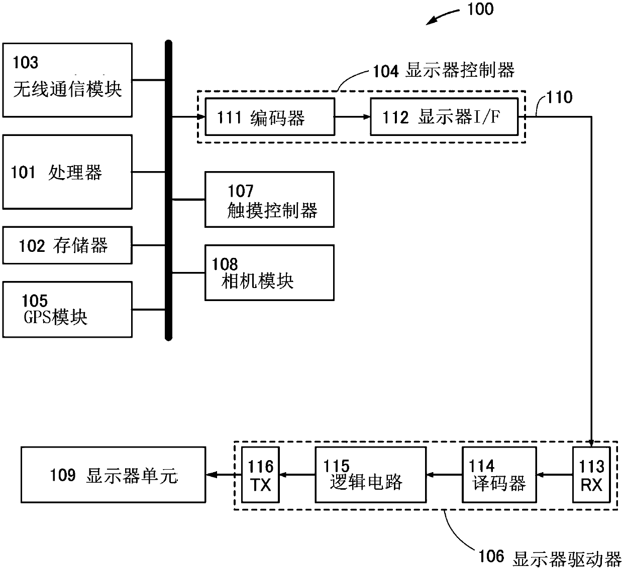
[0042] figure 1 The configuration of the electronic device system described in this embodiment is shown. The electronic device system 100 includes a processor 101 , a memory 102 , a wireless communication module 103 , a display controller 104 , a global positioning system (GPS) module 105 , a display driver 106 , a touch controller 107 , a camera module 108 and a display unit 109 . Display controller 104 is connected to display driver 106 via data bus 110 .
[0043] The display controller 104 includes an encoder circuit 111 and a display interface 112 . In addition, the display driver 106 includes a receiver circuit 113 , a decoder circuit 114 , a logic circuit 115 , and a transceiver circuit 116 .
[0044]Hereinafter, the flow of data displayed on the display unit 109 will be briefly described. Processor 101 processes data stored in memory 102 or data obtained from wireless communication module 103 , GPS module 105 , touch controller 107 , camera module 108 , etc. to gener...
Embodiment approach 2
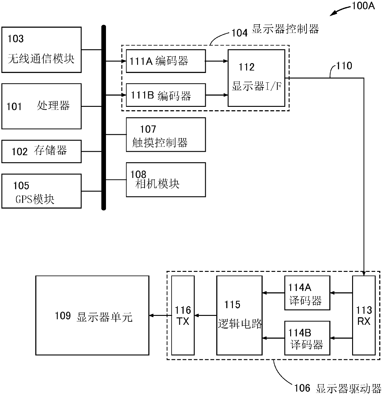
[0076] In Embodiment 1, a mode in which first image data and second image data are sequentially input to one encoder circuit 111 and compressed is shown, but a plurality of encoder circuits and a plurality of decoder circuits may be used.
[0077] exist figure 2 In the illustrated electronic device system 100A, the encoder circuit 111A and the encoder circuit 111B compress the first image data and the second image data, respectively. It is only necessary to fix the compression coefficients for the encoder circuit 111A and the encoder circuit 111B respectively. For example, the compression factor of the encoder circuit 111A may be 1, and the compression factor of the encoder circuit 111B may be 0.5.
[0078] In addition, the electronic device system 100A includes a decoder circuit 114A and a decoder circuit 114B, which respectively decompress the data subjected to the first compression and the data subjected to the second compression. The decoder circuit 114A and the decoder...
Embodiment approach 3
[0081] In Embodiment 2, JPEG formats with different compression coefficients are used when compressing the first image data and the second image data, but formats with different compression formats may be used. For example, the first image data may be compressed in PNG (Portable Network Graphics) format (or the same format) and the second image data may be compressed in JPEG format (or the same format). In addition, the first image data and the second image data may be the same data as in the second embodiment, such as Figure 4B or Figure 4C As shown, there are parts designated as black.
[0082] At this time, in the encoder circuit 111A, first compressed data in the PNG format (or a format similar thereto) is generated from the first image data, and in the encoder circuit 111B, data in the JPEG format ( or the same format as the second compressed data.
[0083] In the decoder circuit 114A, the first compressed data in the PNG format (or the same format) is decompressed t...
PUM
 Abstract
Description
Claims
Application Information
 - R&D Engineer
- R&D Manager
- IP Professional
- Industry Leading Data Capabilities
- Powerful AI technology
- Patent DNA Extraction
Browse by: Latest US Patents, China's latest patents, Technical Efficacy Thesaurus, Application Domain, Technology Topic.
© 2024 PatSnap. All rights reserved.Legal|Privacy policy|Modern Slavery Act Transparency Statement|Sitemap