Chip reliability designing method and device

A reliability and chip technology, applied in the field of chip reliability design, can solve problems such as insufficient reliability analysis, and achieve the effects of avoiding reliability problems, reducing costs, and improving circuits

Inactive Publication Date: 2018-03-16
BEIJING CHIP IDENTIFICATION TECH CO LTD +3
View PDF7 Cites 2 Cited by
  • Summary
  • Abstract
  • Description
  • Claims
  • Application Information

AI Technical Summary

Problems solved by technology

[0005] The purpose of the present invention is to provide a method and device for chip reliability design, thereby overcoming the defect of insufficient reliability analysis in the existing chip design process

Method used


Image

  • Chip reliability designing method and device
  • Chip reliability designing method and device
  • Chip reliability designing method and device

Examples


Embodiment Construction

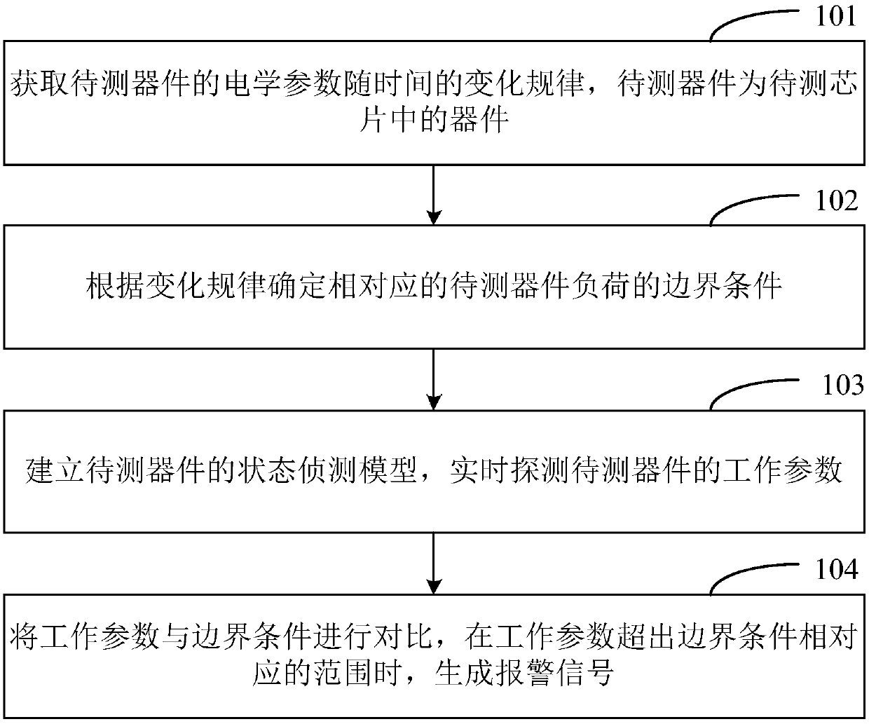
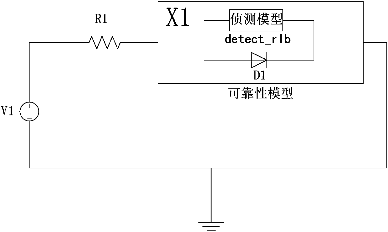
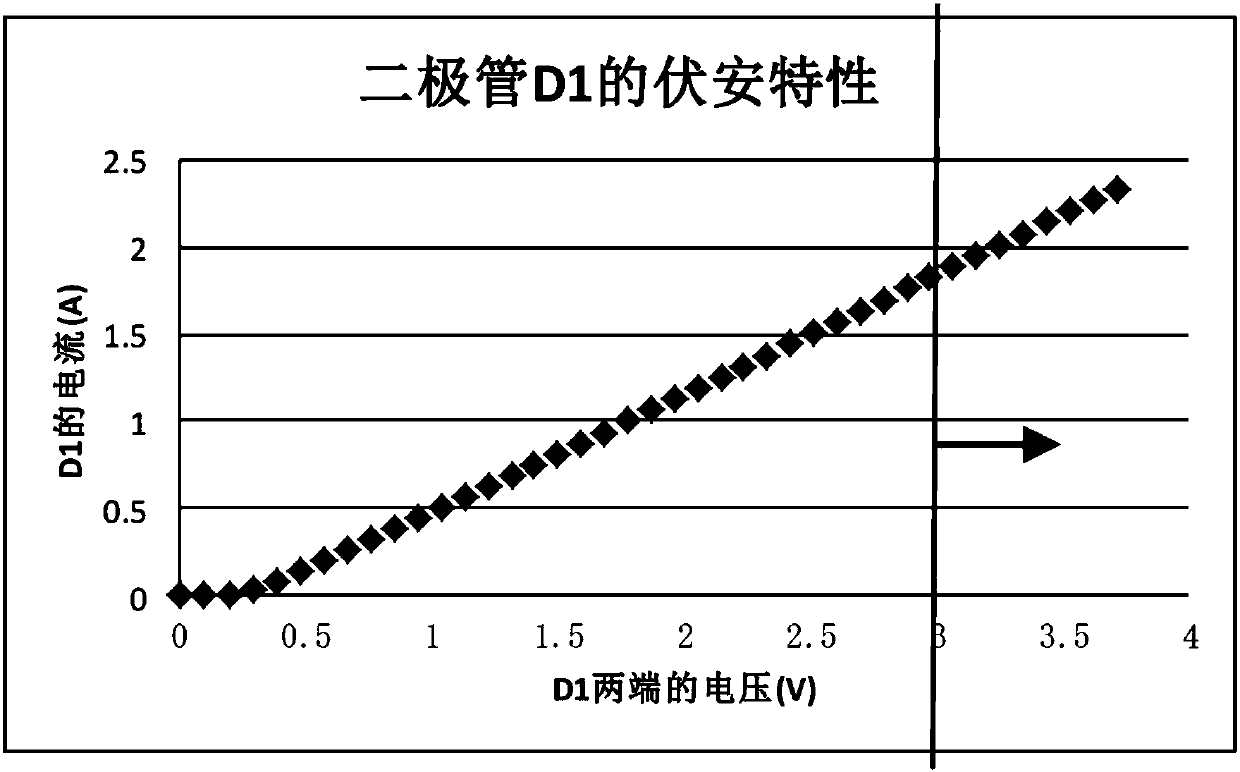
[0023] The specific embodiments of the present invention will be described in detail below in conjunction with the accompanying drawings, but it should be understood that the protection scope of the present invention is not limited by the specific embodiments.

[0024] In order to make the purpose, technical solutions and advantages of the embodiments of the present invention clearer, the technical solutions in the embodiments of the present invention will be clearly and completely described below in conjunction with the drawings in the embodiments of the present invention. Obviously, the described embodiments It is a part of embodiments of the present invention, but not all embodiments. Based on the embodiments of the present invention, all other embodiments obtained by persons of ordinary skill in the art without creative efforts fall within the protection scope of the present invention. Unless expressly stated otherwise, throughout the specification and claims, the term "co...


PUM


Abstract

The invention discloses a chip reliability designing method and device. The method comprises the following steps that: obtaining the change rule of an electrical parameter of a device to be tested along with time, wherein the device to be tested is a device in a chip to be tested; according to the change rule, determining the boundary condition loaded by a corresponding device to be tested; establishing the state detection model of the device to be tested, and detecting the working parameter of the device to be tested in real time; and comparing the working parameter with the boundary condition, and generating an alarm signal when the working parameter exceeds a range corresponding to the boundary condition. By use of the method, reliability design is imported in a chip design stage, and alink with weak reliability is detected to improve a circuit and prolong the service life of the chip.

Description

technical field [0001] The invention relates to the technical field of chip design, in particular to a method and device for chip reliability design. Background technique [0002] Today, with the rapid development of science and technology, electronic information technology based on microelectronics technology has set off a new technological revolution. With the continuous development of large-scale integrated circuits, especially the continuous advancement of silicon integrated circuit technology to sub-micron and even deep sub-micron, the degree of circuit integration and cost performance have been continuously improved. High performance, density and reliability are the key to the development of large-scale integrated circuits. Directions and goals, the main reasons are as follows: 1. The improvement of integration can improve the performance of devices and circuits, and at the same time reduce the price of a single product, which is the driving force behind the developmen...

Claims


Application Information

Patent Timeline
Patent Type & Authority Applications(China)
IPC IPC(8): G06F17/50
CPCG06F30/367
Inventor 付振陈燕宁袁远东张海峰李书振李建强刘芳马强裴万里张虹
Owner BEIJING CHIP IDENTIFICATION TECH CO LTD
Why Eureka
Try Eureka