Display device, display substrate and display compensation method and device

A technology of display substrate and compensation method, applied in static indicators, instruments, etc., can solve the problems of poor display effect, driving transistor threshold voltage drift, uneven product display, etc., and achieve the effect of eliminating traces and good display effect.

Active Publication Date: 2018-05-18
BOE TECH GRP CO LTD
View PDF8 Cites 9 Cited by
  • Summary
  • Abstract
  • Description
  • Claims
  • Application Information

AI Technical Summary

Problems solved by technology

For example, due to reasons such as technology, materials, and design, the threshold voltage of the drive transistor in the AMOLED product drifts, which in turn causes uneven display and poor display effect.

Method used


Image

  • Display device, display substrate and display compensation method and device
  • Display device, display substrate and display compensation method and device
  • Display device, display substrate and display compensation method and device

Examples


Embodiment Construction

[0037] Embodiments of the present invention are described in detail below, examples of which are shown in the drawings, wherein the same or similar reference numerals designate the same or similar elements or elements having the same or similar functions throughout. The embodiments described below by referring to the figures are exemplary and are intended to explain the present invention and should not be construed as limiting the present invention.

[0038] A display compensation method, a display compensation device, a display substrate, and a display device according to embodiments of the present invention will be described below with reference to the accompanying drawings.

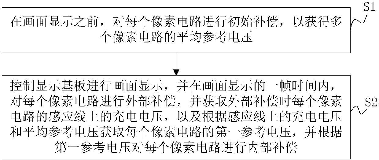
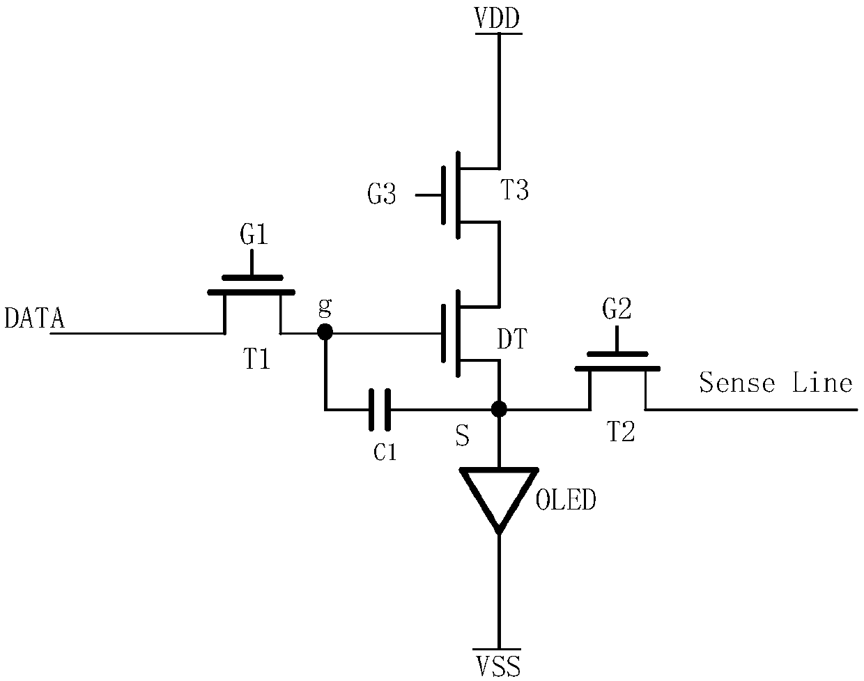
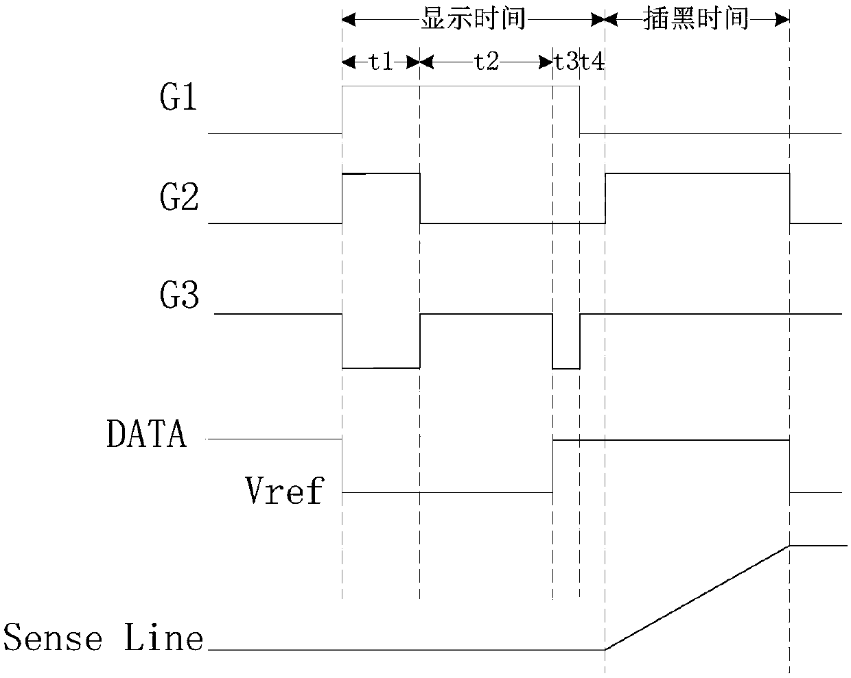
[0039] Usually, when manufacturing display products (such as AMOLED products), due to reasons such as technology, materials, and design, the threshold voltage of the driving transistor in the display product drifts, which in turn causes the problem of uneven display and poor display effect.

[0040] In...


PUM


Abstract

The invention discloses a display device, a display substrate and a display compensation method and device. The method comprises the following steps: before an image is displayed, performing initial compensation on each pixel circuit to obtain the average reference voltage of a plurality of pixel circuits; controlling the display substrate to display the image, and performing external compensationon each pixel circuit within the display time of a frame of the image, and acquiring the charging voltage of the sensing line of each pixel circuit during the external compensation, acquiring the first reference voltage of each pixel circuit according to the charging voltage of the sensing lines and the average reference voltage, and performing internal compensation on each pixel circuit according to the first reference voltage. Thus, not only can threshold voltage compensation of a driving transistor be realized, but also a large characteristic change of the driving transistor can be covered and real-time compensation is performed on the characteristic change of the driving transistor. Further, traces generated by external compensation can be eliminated so that the display effect can befurther improved.

Description

technical field [0001] The present invention relates to the field of display technology, in particular to a display compensation method, a display compensation device, a display substrate and a display device. Background technique [0002] With the advancement of time, AMOLED (Active Matrix Organic Light Emitting Diode, active matrix organic light emitting diode) products are more and more widely used, with its advantages of high contrast, high color gamut, light and thin, and can be made into flexible screens. , is increasingly recognized by people. [0003] With the widespread use of AMOLED products, some problems in the display process need to be properly resolved. For example, due to reasons such as technology, materials, and design, the threshold voltage of the drive transistor in the AMOLED product drifts, which in turn leads to uneven display and poor display effect. Contents of the invention [0004] The present invention aims to solve one of the technical proble...

Claims


Application Information

Patent Timeline
Patent Type & Authority Applications(China)
IPC IPC(8): G09G3/3258
CPCG09G3/3258G09G3/3233G09G2320/0233G09G2320/0295G09G2320/043G09G2300/0819G09G2320/045
Inventor 盖翠丽张保侠王玲徐攀林奕呈
Owner BOE TECH GRP CO LTD
Why Eureka
Try Eureka