
Lead processing device and semiconductor device manufactured using the same

A technology for processing equipment and semiconductors, which is applied in the fields of semiconductor devices, semiconductor/solid-state device manufacturing, and semiconductor/solid-state device components, etc., and can solve the problems of inability to remove connecting rods and resin burrs.

Active Publication Date: 2022-01-14
MITSUBISHI ELECTRIC CORP
View PDF10 Cites 0 Cited by
  • Summary
  • Abstract
  • Description
  • Claims
  • Application Information

AI Technical Summary

Problems solved by technology

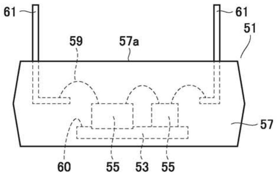
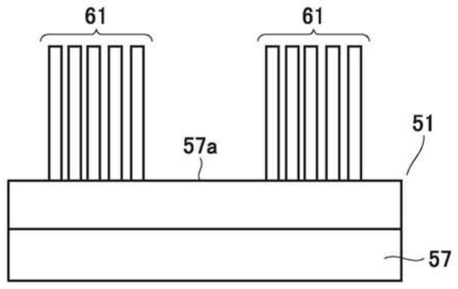
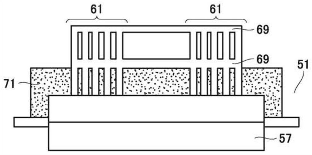
[0008] However, there is a problem that, in the case of a resin-molded semiconductor device in which the external terminals protrude from the upper surface of the resin-encapsulated body, the connection bar cannot be removed by a lead processing device capable of moving the punch in the vertical direction. and resin flash

Method used


Image

  • Lead processing device and semiconductor device manufactured using the same
  • Lead processing device and semiconductor device manufactured using the same
  • Lead processing device and semiconductor device manufactured using the same

Examples


Embodiment approach 1

[0086] First, the basic concept of the lead processing device according to Embodiment 1 will be described using schematic diagrams. Such as Figure 14 As shown, in the lead processing device 1, the resin-molded semiconductor device 51 is arranged such that the surface 57a of the sealing resin body 57 faces upward, and the direction (first direction) in which the external terminal 61 protrudes from the surface 57a becomes upward ( Encapsulation resin body 57). The template 5 is inserted between the opposing external terminal 61 and the other external terminal 61 , and the template 5 is arranged to face the external terminal 61 on the side of the external terminal 61 .

[0087] Moreover, the release plate 7 is arrange|positioned so that it may oppose the plate|plate 5 with a distance from the external terminal 61. As shown in FIG. Here, the template 5 and the release plate 7 are arranged so that a gap is provided between the template 5 and the external terminal 61 , and a gap ...

Embodiment approach 2

[0125] First, the basic concept of the lead processing device according to Embodiment 2 will be described using schematic diagrams. Such as Figure 29 As shown, in the lead processing device 1, the resin-molded semiconductor device 51 is arranged such that the surface 57a of the sealing resin body 57 faces upward, and the direction (first direction) in which the external terminal 61 protrudes from the surface 57a becomes upward ( Encapsulation resin body 57). The template 5 and the release plate 7 are arranged so that the external terminals 61 are sandwiched between the template 5 and the release plate 7 to pressurize the resin-molded semiconductor device 51 that has been placed.

[0126] In this state, the connecting rod 69 and the resin burr 71 are cut off by moving the punch 41 toward the template 5 in a direction intersecting with the protruding direction of the external terminal 61 (second direction). An insertion hole 5a through which the punch 41 is inserted to discha...

Embodiment approach 3

[0145] First, the basic concept of the lead processing device according to Embodiment 3 will be described using schematic diagrams. Such as Figure 35 As shown, in the lead wire processing device 1, the resin package is arranged such that the surface 57a of the package resin body 57 faces the lateral direction, and the direction (first direction) in which the external terminal 61 protrudes from the surface 57a becomes the lateral direction (X-axis negative direction). type semiconductor device 51 (encapsulating resin body 57). The template 5 is inserted between the opposing external terminal 61 and the other external terminal 61 , and the template 5 is arranged to face the external terminal 61 directly below or directly above the external terminal 61 . The release plate 7 is disposed so as to sandwich the external terminal 61 with the plate 5 .

[0146] In this state, the connecting rod 69 and the resin burr 71 are cut off by moving the punch 41 toward the die plate 5 in a d...


PUM


Abstract

In the lead processing device (1), the semiconductor device (51) is arranged with the surface (57a) of the encapsulating resin body (57) facing upward, and the protruding direction of the external terminal (61) is upward. A template (5) is inserted between one external terminal (61) and the other external terminal (61). The release plate (7) is arranged opposite to the form plate (5). In this state, the punch (41) is moved toward the template (5) in a direction intersecting the protruding direction of the external terminal (61), thereby cutting off the connecting rod (69) and the like. An insertion hole (5a) through which a punch (41) is inserted is formed in the template (5).

Description

technical field [0001] The present invention relates to a lead processing device and a semiconductor device manufactured using the lead processing device, in particular to a lead processing device for processing a lead and a semiconductor device manufactured using the lead processing device, wherein the lead is packaged from a semiconductor element The encapsulating resin body protrudes. Background technique [0002] As a semiconductor device, there is a resin-encapsulated semiconductor device in which a semiconductor element (semiconductor chip) is packaged with a resin. In such a semiconductor device, first, after mounting a semiconductor element on a lead frame, the semiconductor element is packaged by filling the resin encapsulation mold with a resin using a resin encapsulation mold such as transfer molding. [0003] Then, with respect to the lead frame in which the semiconductor element was resin-encapsulated, lead processing is performed by a lead processing device. ...

Claims


Application Information

Patent Timeline
Patent Type & Authority Patents(China)
IPC IPC(8): H01L21/67H01L21/56H01L23/31
CPCH01L21/566H01L21/67092H01L23/3107H01L2924/181B21D28/02B29C45/14262B29C45/14639B29C45/332B29C33/00B29C33/123B26D1/09B29C39/10B29C39/26H01L21/67H01L2224/48091H01L2224/48137H01L2224/48247H01L2224/49171B26F1/40H01L21/4842H01L23/49551H01L2924/00014H01L2924/00012H01L21/67144H01L21/4821H01L21/4846H01L23/49811H01L23/28
Inventor 上田哲也亦贺慎二坂本健
Owner MITSUBISHI ELECTRIC CORP
Learn More