Semiconductor device and method for manufacturing semiconductor element

A manufacturing method and semiconductor technology, applied in the direction of semiconductor/solid-state device manufacturing, semiconductor devices, semiconductor/solid-state device components, etc., to achieve the effect of component trace suppression

Pending Publication Date: 2021-03-26
MITSUBISHI ELECTRIC CORP
View PDF2 Cites 0 Cited by
  • Summary
  • Abstract
  • Description
  • Claims
  • Application Information

AI Technical Summary

Problems solved by technology

However, when evaluating the electrical characteristics of unsingulated semiconductor elements formed on a semiconductor substrate, the above-mentioned problems arise.

Method used


Image

  • Semiconductor device and method for manufacturing semiconductor element
  • Semiconductor device and method for manufacturing semiconductor element
  • Semiconductor device and method for manufacturing semiconductor element

Examples


Embodiment approach 1

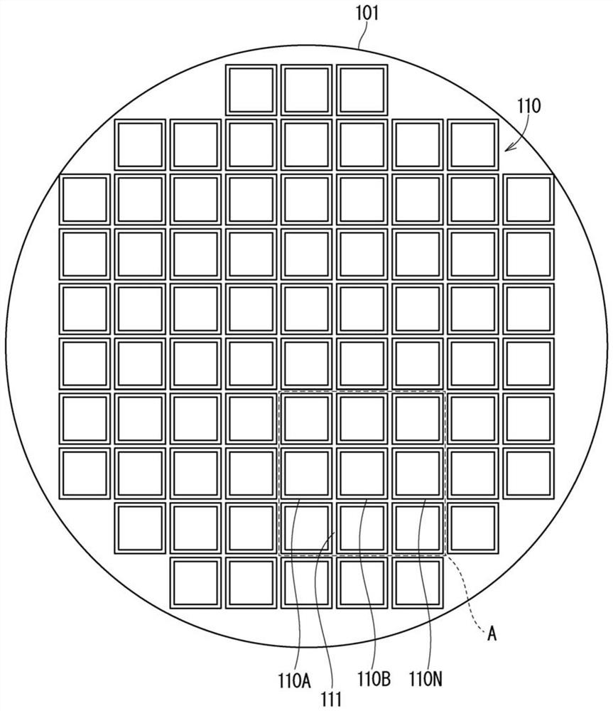
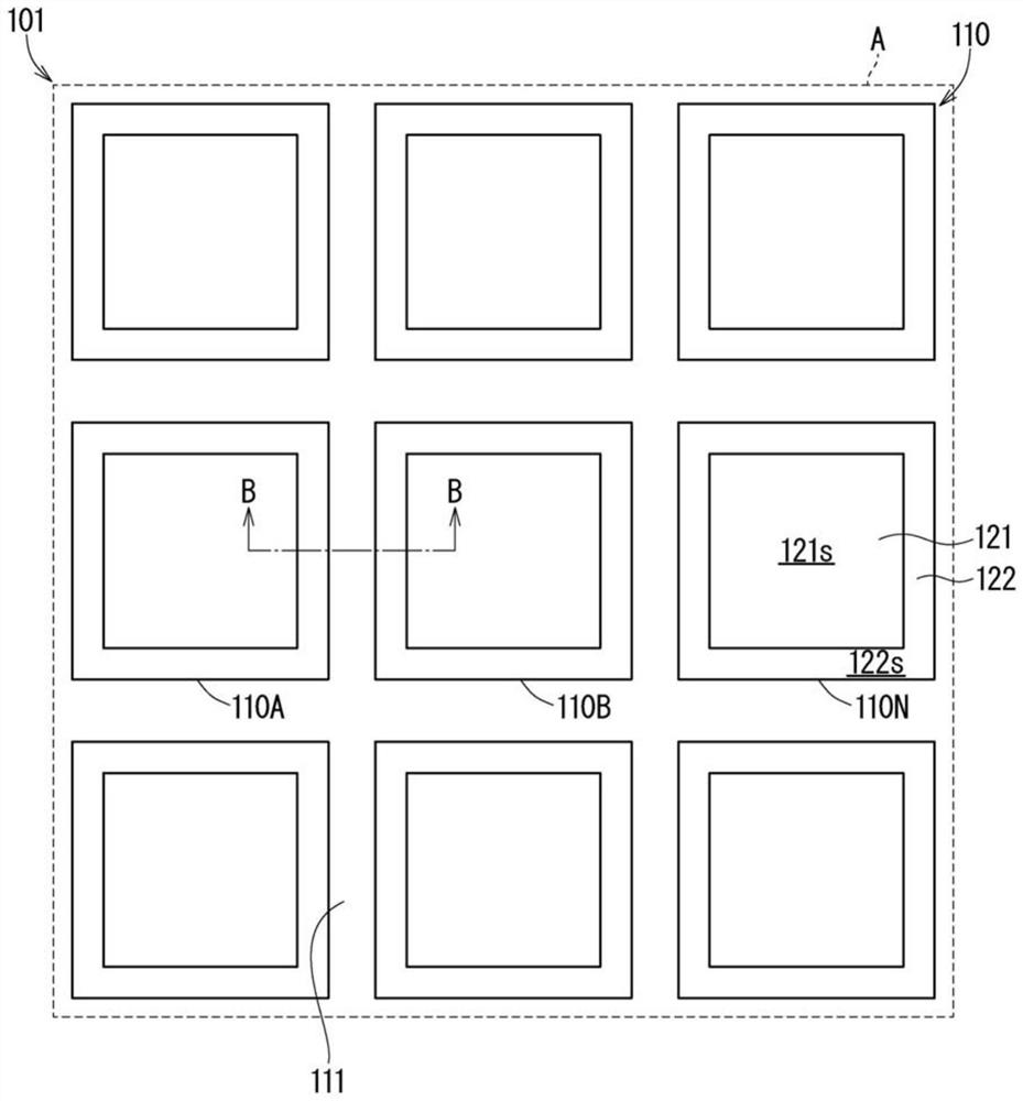
[0047] 1.1 Plane structure of semiconductor substrate

[0048] figure 1 It is a plan view schematically illustrating a semiconductor substrate included in the semiconductor device of the first embodiment. figure 2 It is an enlarged plan view schematically showing a part of the semiconductor substrate included in the semiconductor device according to the first embodiment. figure 2 right figure 1 Part A depicted in is shown enlarged.

[0049] figure 1 as well as figure 2 The illustrated semiconductor substrate 101 has a plurality of semiconductor elements 110 and inter-element portions 111 .

[0050] The plurality of semiconductor elements 110 are arranged in the direction in which the semiconductor substrate 101 spreads. exist figure 1 as well as figure 2 In the semiconductor substrate 101 shown, a plurality of semiconductor elements 110 are arranged in a matrix. The plurality of semiconductor elements 110 are formed by forming p-type diffusion layers, n-type diffu...

Embodiment approach 2

[0098] Figure 11 It is a flowchart illustrating the manufacturing method of the semiconductor element of the second embodiment.

[0099] The method of manufacturing a semiconductor element according to Embodiment 2 has Figure 11 Steps S1 to S6 are shown.

[0100] In step S1, the semiconductor substrate 101 is prepared.

[0101] When preparing the semiconductor substrate 101, a semiconductor wafer is prepared.

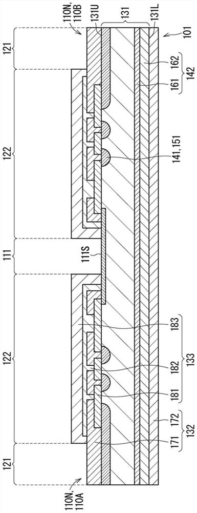
[0102] In addition, impurities are implanted into the prepared semiconductor wafer, and the prepared semiconductor wafer is heated. As a result, the p-type diffusion layer 141 and the n-type diffusion layer 142 are formed on the semiconductor wafer to obtain image 3 A semiconductor wafer 131 is shown.

[0103] In addition, electrodes 132 and an insulating layer 133 are formed on the obtained semiconductor wafer 131 . From this, get image 3 A semiconductor substrate 101 is shown.

[0104] The obtained semiconductor substrate 101 has a plurality of semiconduct...


PUM

PropertyMeasurementUnit
glass transition temperatureaaaaaaaaaa

Abstract

Disclosed are a semiconductor device, and a method for manufacturing semiconductors. When a voltage is applied to a semiconductor element formed into a semiconductor substrate for evaluating the electrical characteristic of the semiconductor element, partial discharge between the semiconductor element and an inter-element portion, adhesion of a foreign substance to the semiconductor substrate, andformation of a trace of a component in the semiconductor substrate are prevented. A semiconductor device includes a semiconductor substrate and a discharge inhibitor. The semiconductor substrate includes a plurality of semiconductor elements and an inter-element portion. The semiconductor elements are arranged in a spreading direction of the semiconductor substrate. The inter-element portion is between adjacent semiconductor elements among the semiconductor elements. The discharge inhibitor is bonded not to a surface of a center of each semiconductor element among the semiconductor elements but to a surface of the inter-element portion. The discharge inhibitor is made of an insulator.

Description

technical field [0001] The present invention relates to a method of manufacturing a semiconductor device and a semiconductor element. Background technique [0002] In many cases, a chip-shaped semiconductor element is manufactured by forming a plurality of semiconductor elements on a semiconductor substrate and singulating the formed plurality of semiconductor elements. [0003] When evaluating the electrical characteristics of semiconductor elements when manufacturing chip-shaped semiconductor elements, the electrical characteristics of the singulated semiconductor elements are sometimes evaluated, and sometimes the electrical characteristics of the unsingulated semiconductor elements formed on the semiconductor substrate are evaluated. The electrical characteristics of semiconductor elements are evaluated. [0004] When evaluating the electrical characteristics of the singulated semiconductor element, the installation surface of the semiconductor element to be evaluated i...

Claims


Application Information

Patent Timeline
Patent Type & Authority Applications(China)
IPC IPC(8): H01L23/60H01L21/78
CPCH01L23/60H01L21/78H01L22/30H01L25/072H01L25/50H01L22/14H01L21/02282H01L21/02118
Inventor 野村典嗣
Owner MITSUBISHI ELECTRIC CORP
Why Eureka
Try Eureka