Test key of COA substrate and testing method using test key of COA substrate

A technology for testing keys and substrates, which is applied in nonlinear optics, instruments, optics, etc., can solve the problems of long production cycle time and large occupied space, and achieve increased available space, small occupied space, and reduced production cycle time Effect

Active Publication Date: 2018-06-22
TCL CHINA STAR OPTOELECTRONICS TECH CO LTD
View PDF10 Cites 9 Cited by
  • Summary
  • Abstract
  • Description
  • Claims
  • Application Information

AI Technical Summary

Problems solved by technology

[0003] At present, the test key for the line width of the via hole in the RGB color-resistive layer and the test key for the alignment accuracy between the RGB color-resistive layer and the thin film transistor layer are independently designed patterns. This design takes up a large space, and the above-mentioned In the two measurements, it is necessary to move the lens of the test device to measure the alignment accuracy of the RGB color-resistive layer and the thin-film transistor layer after the test key of the via line width of the RGB color-resistive layer, which leads to production beats longer time

Method used


Image

  • Test key of COA substrate and testing method using test key of COA substrate
  • Test key of COA substrate and testing method using test key of COA substrate

Examples


Embodiment Construction

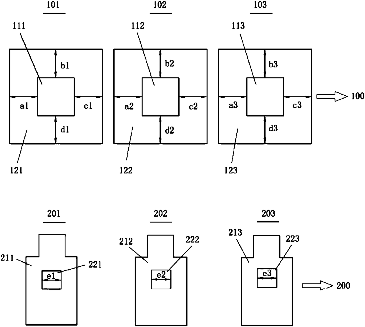
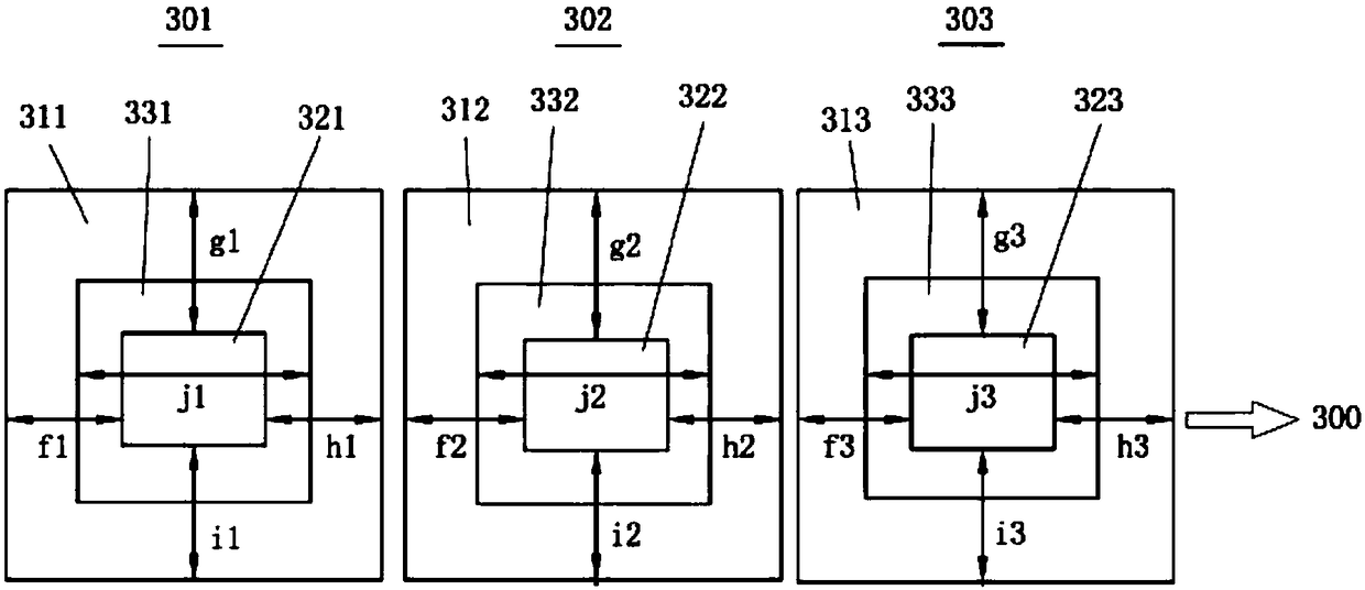
[0018] Hereinafter, the inventive concept will be described in detail by explaining exemplary embodiments with reference to the accompanying drawings. However, the inventive concepts may be embodied in many different forms and should not be construed as limited to the embodiments set forth herein; rather, these embodiments are provided so that this disclosure will be thorough and complete, and will inform the present Those of ordinary skill in the art fully convey the inventive concept. In the drawings, the same reference numerals denote the same elements. Furthermore, various elements and regions are shown schematically. Accordingly, the inventive concepts are not limited to the relative sizes or distances shown in the drawings. It will be understood that although the terms first, second etc. may be used herein to describe various elements and / or components, these elements and / or components should not be limited by these terms. These terms are only used to distinguish one ...


PUM


Abstract

The invention provides a test key of a COA substrate and a testing method using the test key of the COA substrate. The test key of the COA substrate comprises a first test key, a second test key and athird test key, wherein the first test key comprises a red color resistance pattern, a first via hole pattern formed in the red color resistance pattern and a first metal layer pattern, the second test key comprises a green color resistance pattern, a second via hole pattern formed in the green color resistance pattern and a second metal layer pattern, the third test key comprises a blue color resistance pattern, a third via hole pattern formed in the blue color resistance pattern and a third metal layer pattern, and the first metal layer pattern, the second metal layer pattern and the thirdmetal layer pattern are formed from a same metal layer. The test key of the COA substrate occupies smaller space, and the alignment precision of a color resistance layer relative to a thin film transistor layer and the line width of via holes in the color resistance layer can be simultaneously measured.

Description

technical field [0001] The invention relates to the technical field of liquid crystal displays, in particular to a test key of a COA substrate and a test method using the test key of the COA substrate. Background technique [0002] The COA (Color Filter on Array) substrate of the existing Thin Film Transistor Liquid Crystal Display (TFT-LCD, Thin Film Transistor Liquid Crystal Display) is to manufacture color filters on the thin film transistor array substrate. [0003] At present, the test key for the line width of the via hole in the RGB color-resistive layer and the test key for the alignment accuracy between the RGB color-resistive layer and the thin film transistor layer are independently designed patterns. This design takes up a large space, and the above-mentioned In the two measurements, it is necessary to move the lens of the test device to measure the alignment accuracy of the RGB color-resistive layer and the thin-film transistor layer after the test key of the vi...

Claims


Application Information

Patent Timeline
Patent Type & Authority Applications(China)
IPC IPC(8): G02F1/1362
CPCG02F1/1362G02F1/136222G02F1/136254
Inventor 何伟
Owner TCL CHINA STAR OPTOELECTRONICS TECH CO LTD
Why Eureka
Try Eureka