Array substrate, display screen and display device

An array substrate and substrate technology, applied in static indicators, instruments, etc., can solve the problem of uneven brightness of displayed images, achieve the effect of improving display effect, increasing parasitic capacitance, and solving uneven brightness of images

Active Publication Date: 2018-08-17
KUNSHAN GO VISIONOX OPTO ELECTRONICS CO LTD
View PDF7 Cites 25 Cited by
  • Summary
  • Abstract
  • Description
  • Claims
  • Application Information

AI Technical Summary

Problems solved by technology

[0005] Based on this, it is necessary to provide an array substrate, a display screen and a display device to solve the technical problem of uneven brightness of the displayed image caused by the difference in the number of pixels between the special-shaped display area and the non-special-shaped display area in the traditional technology.

Method used


Image

  • Array substrate, display screen and display device
  • Array substrate, display screen and display device
  • Array substrate, display screen and display device

Examples


Embodiment Construction

[0025] In order to make the above objects, features and advantages of the present invention more comprehensible, specific implementations of the present invention will be described in detail below in conjunction with the accompanying drawings. In the following description, numerous specific details are set forth in order to provide a thorough understanding of the present invention. However, the present invention can be implemented in many other ways different from those described here, and those skilled in the art can make similar improvements without departing from the connotation of the present invention, so the present invention is not limited by the specific embodiments disclosed below.

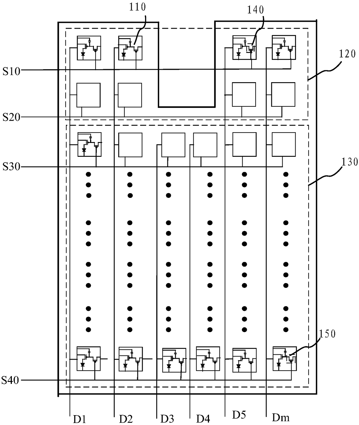
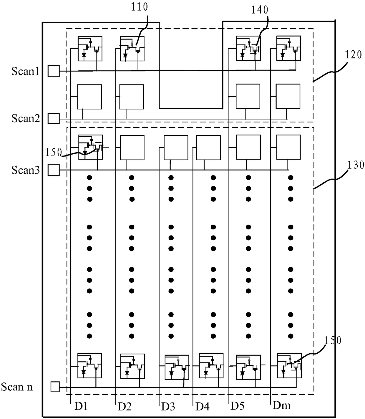
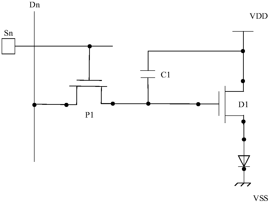
[0026] In one embodiment, see figure 1 The present application provides an array substrate. The array substrate includes a substrate. The corresponding display area on the substrate includes pixels 110 arranged in an array. The display area is divided into a special-shaped display area 12...


PUM


Abstract

The invention relates to an array substrate, a display screen and a display device. The array substrate comprises a substrate body, at least one first switch transistor and at least one second switchtransistor, a corresponding display area on the substrate body comprises pixels in array distribution and is divided into a special-shaped display area and a non-special-shaped display area, the number of the pixels in each row of the special-shaped display area is smaller than that in any row of the non-special-shaped display area, the first switch transistors are positioned in the special-shapeddisplay area and correspond to the pin the special-shaped display area, and the second switch transistors are positioned in the non-special-shaped display area and correspond to the pixels in the non-special-shaped display area; width-length ratio of the first switch transistors is equal to that of the second switch transistor, and grid area of the first switch transistors is greater than that ofthe second switch transistors. The technical problem that displayed images are nonuniform in brightness caused by load difference in the special-shaped display area and the non-special-shaped displayarea is solved, and display effect is improved.

Description

technical field [0001] The present invention relates to the field of display technology, in particular to an array substrate, a display screen and a display device. Background technique [0002] At present, the display screens of common display devices, such as monitors, televisions, mobile phones, tablet computers, etc., are usually regular rectangles. With the development of display technologies, rectangular display screens can no longer meet the diverse needs of users. Therefore, the shapes of display screens are becoming more and more diverse. [0003] Generally, a non-rectangular display is called a shaped display. The special-shaped display screen includes a special-shaped display area and a non-special-shaped display area. The number of pixels per row in the special-shaped display area is different from the number of pixels per row in the non-special-shaped display area. [0004] In the conventional technology, the driving circuit in the display panel controls the...

Claims


Application Information

Patent Timeline
Patent Type & Authority Applications(China)
IPC IPC(8): G09G3/20
CPCG09G3/20G09G2310/0267
Inventor 朱正勇贾溪洋朱晖
Owner KUNSHAN GO VISIONOX OPTO ELECTRONICS CO LTD
Why Eureka
Try Eureka