Interconnection line structure and forming method thereof

An interconnection wire and semiconductor technology, applied in the field of interconnection wire structure and the formation of interconnection wire structure, can solve the problems of small parasitic capacitance and the effect of parasitic capacitance is no longer obvious, and achieve the reduction of parasitic capacitance and dielectric constant Small, improve the effect of RC delay

Active Publication Date: 2013-05-01
SHANGHAI HUAHONG GRACE SEMICON MFG CORP
View PDF5 Cites 11 Cited by
  • Summary
  • Abstract
  • Description
  • Claims
  • Application Information

AI Technical Summary

Problems solved by technology

However, when the process technology enters below 32nm, the role of the low-dielectric material in reducing parasitic capacitance is no longer obvious
Moreover, even for technologies with larger process nodes above 90nm, the existing method of completely filling the trenches between adjacent metal interconnection lines with the intermetallic dielectric layer cannot meet the requirements for the gap between adjacent metal interconnection lines. Minimize the parasitic capacitance between the technical requirements, such as some radio frequency integrated circuits

Method used


Image

  • Interconnection line structure and forming method thereof
  • Interconnection line structure and forming method thereof
  • Interconnection line structure and forming method thereof

Examples


Embodiment Construction

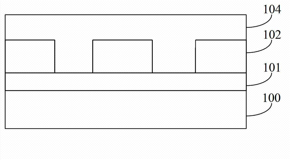
[0037] The inventor researched the existing metal interconnection structure forming method and found that, referring to Figure 4 , as the distance between adjacent metal interconnection lines becomes smaller, an air gap 105 is formed in the intermetallic dielectric layer 104 between adjacent metal interconnection lines. The inventor further studied the problem of the air gap, and realized that the air gap 105 will not increase the parasitic capacitance between adjacent metal interconnection lines, but will reduce the parasitic capacitance. Forming an air gap (air gap) between adjacent metal interconnection lines can be used as an effective method to reduce parasitic capacitance between metal interconnections.

[0038] Therefore, how to form an air gap in the intermetallic dielectric layer between adjacent metal interconnection lines, or even form a larger volume of air gap, has become the research focus of the inventors.

[0039] Through creative work, the inventor obtained ...


PUM


Abstract

The invention provides an interconnection line structure and a forming method of the interconnection line structure. The forming method of the interconnection line structure comprises the following steps of: providing a semiconductor substrate, wherein a semiconductor device is formed in the semiconductor substrate; forming an interlayer medium layer on the semiconductor substrate; forming a conductive layer on the interlayer medium layer; after the conductive layer is formed, forming grooves in the conductive layer and the interlayer medium layer, wherein the depth of the grooves is less than a thickness sum of the conductive layer and the interlayer medium layer, and a depth-to-width ratio of the grooves is more than 0.8; after the grooves are formed, depositing intermetallic medium layers, covering the conductive layer and filling the grooves through the intermetallic medium layers, and forming air gaps in the intermetallic medium layers. Compared with the prior art, the height of the grooves comprises the height of the conductive layer and a part of the height of the intermetallic medium layers, so that the depth-to-width ratio of the grooves between the adjacent interconnection lines is increased, the air gaps formed in the intermetallic medium layers inside the grooves are larger, stray capacitance is reduced and even removed, and the properties of the semiconductor device can be improved.

Description

technical field [0001] The invention relates to the technical field of semiconductors, in particular to an interconnect structure and a method for forming the interconnect structure. Background technique [0002] Existing methods for forming metal interconnection structures include: [0003] refer to figure 1 A semiconductor substrate 100 is provided, on which a dielectric layer 101 and a metal layer 102 located on the dielectric layer 101 are formed. [0004] refer to figure 2 , form a patterned photoresist layer (not shown) on the metal layer 102, and use the patterned photoresist layer as a mask to etch the metal layer 102 to form a trench 103, and the grooves on both sides of the trench 103 The metal layer 102 also forms a metal interconnection line. [0005] refer to image 3 , deposit an inter-metal dielectric layer 104 , the inter-metal dielectric layer 104 fills the trench 103 and covers the metal layer 102 . [0006] However, when the semiconductor industry e...

Claims


Application Information

Patent Timeline
Patent Type & Authority Applications(China)
IPC IPC(8): H01L21/768H01L23/522
CPCH01L23/53295H01L23/5222H01L23/5226H01L21/76877H01L23/5329H01L21/7682H01L2924/0002H01L2924/00
Inventor 李乐
Owner SHANGHAI HUAHONG GRACE SEMICON MFG CORP
Why Eureka
Try Eureka