Complex microdevices and apparatus and methods for fabricating such devices

a micro-device and complex technology, applied in the direction of acceleration measurement using interia forces, instruments, coatings, etc., can solve the problems of electrostatic devices proposed or developed, monolithic formation, and destructive separation of masking material from the substra

Inactive Publication Date: 2003-10-02
MEMGEN
View PDF14 Cites 130 Cited by
  • Summary
  • Abstract
  • Description
  • Claims
  • Application Information

AI Technical Summary

Benefits of technology

[0167] Some embodiments may use nickel as a structural material while other embodiments may use different materials such as copper, gold, silver, or any other electrodepositable materials that can be separated from the a sacrificial material. Some embodiments may use copper as the structural material with or without a sacrificial material. Some embodiments may remove a sacrificial material while other embodiments may not. In some embodiments the sacrificial material may be removed by a chemical etching operation, an electrochemical operation, or a melting operation. In some embodiments the anode may be different from the conformable contact mask support and the support may be a porous structure or other perforated structure. Some embodiments may use multiple conformable contact masks with different patterns so as to deposit different selective patterns of material on different layers and / or on different portions of a single layer. In some embodiments, the depth of deposition will be enhanced by pulling the conformable contact mask away from the substrate as deposition is occurring in a manner that allows the seal between the conformable portion of the CC mask and the substrate to shift from the face of the conformal material to the inside edges of the conformable material.

Problems solved by technology

The CC mask plating process is distinct from a "through-mask" plating process in that in a through-mask plating process the separation of the masking material from the substrate would occur destructively.
Some of these devices may be formed monolithically in an Electrochemical Fabrication process.
Electrostatic devices proposed or developed have typically suffered from some problems: (1) though electrostatic forces achieved have been sufficient for some applications, they have been inadequate for others; (2) high actuation voltages have typically been necessary, e.g. in excess of 100 volts, and / or (3) some devices have exhibited unpredictable behavior or stiction which may be the result of production of unintended electric fields.
The main issues associated with linear electrostatic actuators actuation force vs. voltage and total displacement or throw.
Limitations of conventional high-aspect ratio processing generally have required an increased comb gap at greater etch depths which have somewhat reduced the advantages of using high aspect ratio structures.
These actuators typically produce higher forces than to comb drives but are nonlinear in their operation.
This can be a problem when a large range of motion is required.
Unfortunately, this often requires the electrode to be placed at a substantial distance from the moving member, which drastically reduces the available force.
It then becomes difficult to initiate motion in the moving member.
As a result, tilt mirror devices for example typically require large operating voltages due to the large distance between the mirror and electrode.
Furthermore, this conventional approach results in a very nonlinear actuator behavior, requiring use of complex control schemes to compensate for the increase in force as the gap closes.
Microfluidic systems often require complex networks of wells and channels for their operation.

Method used


Image

  • Complex microdevices and apparatus and methods for fabricating such devices
  • Complex microdevices and apparatus and methods for fabricating such devices
  • Complex microdevices and apparatus and methods for fabricating such devices

Examples


first embodiment

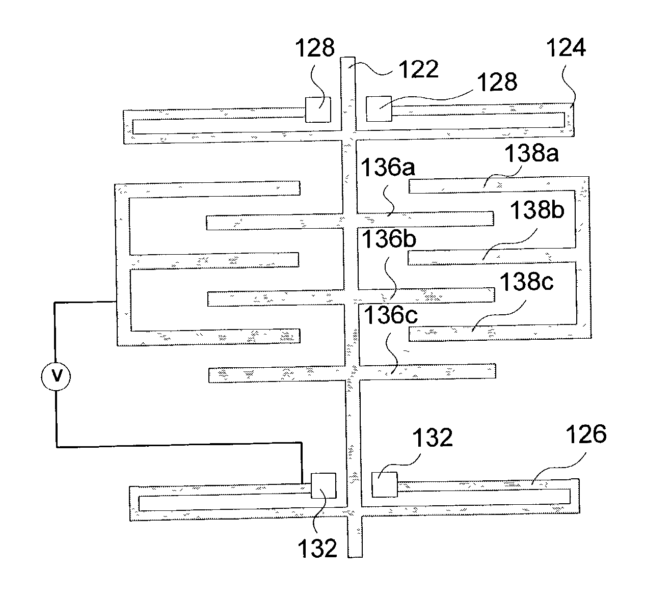
[0111] FIG. 4 illustrates a pressure sensor according to a This pressure sensor includes a plurality of stacked capacitor plates that may by used to enhance the sensitivity of any displacement caused by a pressure differential. The pressure sensor of the present embodiment includes a base plate 102 through which conductive leads 104 and 106 extend. Conductive lead 106 connects to walls 108 and flexible lid member 112 when a pressure P is exerted on the outside lid member 112 which exceeds a pressure P inside a chamber 114 formed by base 102 walls 108 and lid 112, a downward deflection of lid 112 occurs which causes a deflection of capacitive plates 116(a), 116(b) and 116(c) relative to capacitive plates 118(a), 118(b), and 118(c). This deflection causes a change in the capacitance of the capacitor that is formed by set of plates 116(a)-116(c) and 118(a)-118(c). This change in capacitance can be detected and correlated to a pressure differential. Due to the existence of multiple cap...

third embodiment

[0116] the invention is depicted in FIGS. 6(a)-6(c). FIG. 6(a) depicts a perspective view of the moving portion of an actuator while FIG. 6(b) depicts an expanded view of a portion of the structure of FIG. 6(a) such that individual capacitor plates can be seen in several of the stacks. FIG. 6(c) depicts a top view of both the moving elements and the fixed elements of the actuator of FIGS. 6(a) and 6(b). The moving elements of actuator 6(a) include a plurality of stacks 142a-142r of capacitor plates where each stack itself includes a plurality of capacitor plates as illustrated in FIG. 6(b) as 142a(1), 142a(2), 142a(3), etc. The moving elements also include a shaft 144 and columns 146 that connect all of the capacitor plates into a single structure. Shaft 144 is supported by spring-like elements 148 and 150 which in turn have one end 152 and 154 connected to columns 156 and 158 that extend to a frame (not shown). For clarity of presentation FIGS. 6(a) and 6(b) do not depict the plura...

fourth embodiment

[0117] the present invention provides a linear variable differential transformer or LVDT which may be monolithically produced by electrochemical fabrication. As indicated in FIG. 7, the LVDT may consist of a primary transformer coil 180 and two secondary transformer coils 182a and 182b. Additionally, an armature of magnetically permeable material is included that may move back and forth such that different amounts of the armature may be located in secondary coils 182a or 182b. Armature 184 may have a non-magnetically permeable extension extending out of one or both ends of the secondary coils as indicated by reference numbers 186a and 186b. In use, the LVDT may be supplied with a voltage V1 on primary coils 180 and a voltage difference V2 between the two secondary coils may be detected, to yield a value which can be related to the position of armature 184. Armature 184 is connected via elements 186a or 186b to a structure whose position is to be measured. The detected voltage V2 may...


PUM

PropertyMeasurementUnit
Aspect Ratioaaaaaaaaaa
actuation voltagesaaaaaaaaaa
thicknessaaaaaaaaaa

Abstract

Various embodiments of the invention are directed to various microdevices including sensors, actuators, valves, scanning mirrors, accelerometers, switches, and the like. In some embodiments the devices are formed via electrochemical fabrication (EFAB(TM))

Description

[0001] This application claims priority to U.S. Provisional Patent Application No. 60 / 364,261 filed on Mar. 13, 2002; No. 60 / 340,372 filed on Dec. 6, 2001; No. 60 / 379,133 filed on May 7, 2002; No. 60 / 415,371 filed on Oct. 1, 2002; No. 60 / 379,135 filed on May 7, 2002; No. 60 / 379,177 filed on May 7, 2002; No. 60 / 379,182 filed on May 7, 2002; No. ______ filed on Dec. 3, 2002 (corresponding to MEMGen Docket No. P-US021-B-MG, Ser. No. ______ yet to be determined); No. 60 / 379,184 filed on May 7, 2002; No. 60 / 415,374 filed on Oct. 1, 2002; No. 60 / 379,130 filed on May 7, 2002; No. 60 / 392,531 filed on Jun. 27, 2002; No. 60 / 422,007 filed on Oct. 29, 2002; No. 60 / 422,982 filed on Nov. 1, 2002; No. ______ filed on Nov. 26, 2002 (corresponding to MEMGen Docket No. P-US042-B-MG, Ser. No. ______ yet to be determined); No. ______ filed on Nov. 26, 2002 (corresponding to MEMGen Docket No. P-US043-A-MG, Ser. No. ______ yet to be determined); and No. ______ filed on Dec. 3, 2002 (corresponding to MEMG...

Claims


Application Information

Patent Timeline
Patent Type & Authority Applications(United States)
IPC IPC(8): B81C1/00G01P15/00
CPCB81C1/0019B33Y10/00
Inventor BANG, CHRISTOPHER A.COHEN, ADAM L.LOCKARD, MICHAEL S.EVANS, JOHN D.
Owner MEMGEN
Why Eureka
Try Eureka