Semiconductor platform technology

A semiconductor and process technology, applied in the field of semiconductor microelectronics design and manufacture, can solve problems such as compressing the output dynamic range of transistors, meet the requirements of microwave performance and power performance, high collector junction breakdown voltage, and overcome the problem of large parasitic capacitance. Effect

Inactive Publication Date: 2006-06-28
NO 55 INST CHINA ELECTRONIC SCI & TECHNOLOGYGROUP CO LTD
View PDF0 Cites 11 Cited by
  • Summary
  • Abstract
  • Description
  • Claims
  • Application Information

AI Technical Summary

Problems solved by technology

However, the conventional process can only obtain the positive mesa, and the breakdown voltage of the PN junction is lower than that of the planar structure, which compresses the output dynamic range of the transistor.

Method used


Image

  • Semiconductor platform technology
  • Semiconductor platform technology
  • Semiconductor platform technology

Examples


Embodiment Construction

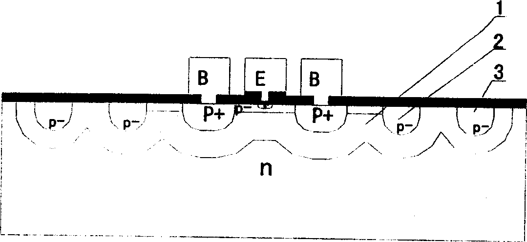
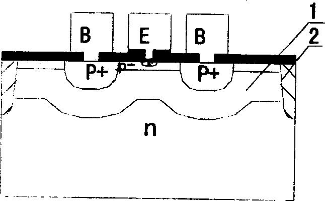
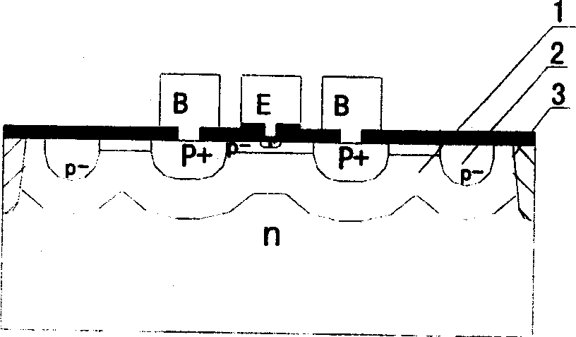
[0059] The present invention will be further described below in conjunction with the accompanying drawings and embodiments.

[0060] Pure semiconductor materials are non-conductive insulators. When a certain impurity element is doped into the semiconductor material, its conductivity will increase by several orders of magnitude, showing good conductivity. For semiconductor silicon, when the doping element is one or more elements in boron, aluminum, etc., it is shown as mobile positively charged particles conduct electricity, and this type of semiconductor is called P-type (p-type) semiconductor. When the dopant element is one or more elements in phosphorus, arsenic, antimony, etc., it behaves as movable negatively charged particles conduct electricity, and this type of semiconductor is called an N-type semiconductor. The higher the concentration of doping elements, the higher the concentration of movable conductive particles, and the stronger the conductivity. Usually use P -...


PUM


Abstract

This invention relates to a platform technology of semiconductors combining advantages of the plane and mesa technologies to diffuse a deep junction at the edge of the PN junction to let it have a most possible high break-over voltage and erode silicon in the width sphere of an exhaust region of the outside of said junction to form a mesa structure, which can bear rather high break-over voltage to block the further expansion of the exhaust areas and reduce the capacitance of the PN junction, so the total break-over voltage of the collector junction of the transistor is increased due to the sum voltage shared by the mesa and the PN junction.

Description

technical field [0001] The invention is a process technology especially suitable for the development and production of microwave power semiconductor diodes and triodes, belonging to the technical field of semiconductor microelectronics design and manufacture. Background technique [0002] The key points and difficulties in the design and manufacture of microwave power transistors mainly include the following three aspects: 1. To overcome the adverse effects of microwave parasitic parameters and improve microwave gain performance. 2. Overcome the large injection effect in the base area, improve the power capacity, and maintain the microwave performance under high-power conditions; 3. Overcome the thermal effect brought by high-power applications, and improve the long-term reliability of the transistor. [0003] In order to expand the output dynamic range and increase the output power of semiconductor transistors, it is required to reduce their saturation voltage drop under ra...

Claims


Application Information

Patent Timeline
Patent Type & Authority Applications(China)
IPC IPC(8): H01L21/331
Inventor 傅义珠
Owner NO 55 INST CHINA ELECTRONIC SCI & TECHNOLOGYGROUP CO LTD
Why Eureka
Try Eureka