

Display panel and display apparatus
A display panel and display area technology, which is applied to identification devices, semiconductor/solid-state device components, instruments, etc., can solve the problems of poor detection effect and low crack detection rate, and achieve intuitive crack detection results, easy identification, and improved The effect of detection efficiency
- Summary
- Abstract
- Description
- Claims
- Application Information
AI Technical Summary
Problems solved by technology
Method used
Image

Examples
Embodiment 1
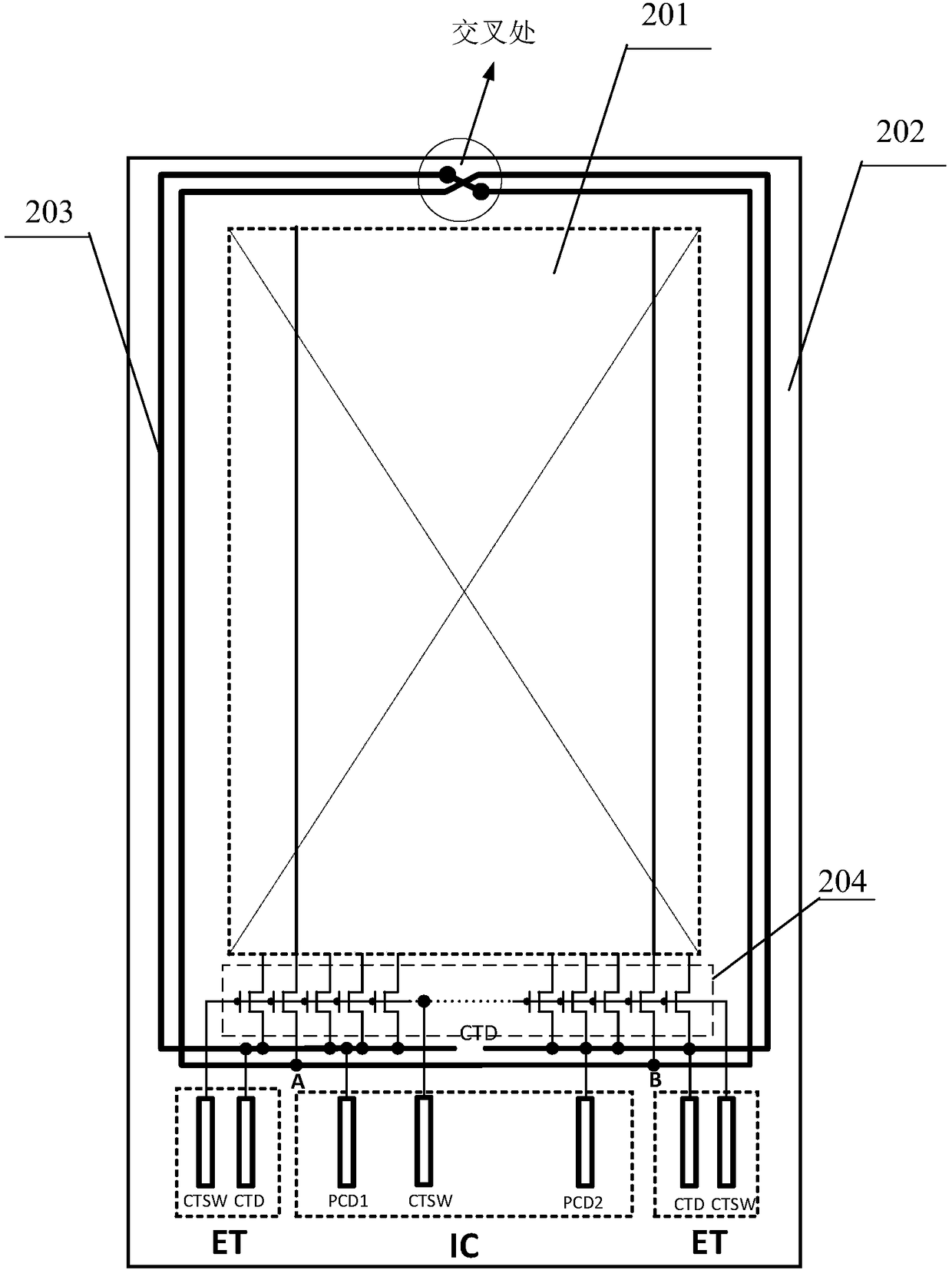
[0041] A structure of a display panel provided by Embodiment 1 of the present invention, such as figure 2 As shown, it includes: a display area 201 and a non-display area 202 surrounding the display area. A metal wire 203 is arranged in the non-display area 202 to form two layers of crack detection wires surrounding the display area 201 .
[0042]Preferably, the start and end of the metal wire 203 are located on the same side of the display panel; for example, as figure 2 As shown, the start and end of the metal wire 203 are both located at the side of the lower end of the display panel.
[0043] An intersection between the inner and outer layers of crack detection wires formed by the metal wire 203 is located on the other side opposite to the side. For example, if figure 2 As shown, the intersection between the inner and outer layers of crack detection wires formed by the metal wire 203 is located in the middle of the upper side of the display panel. The inner and outer...
Embodiment 2
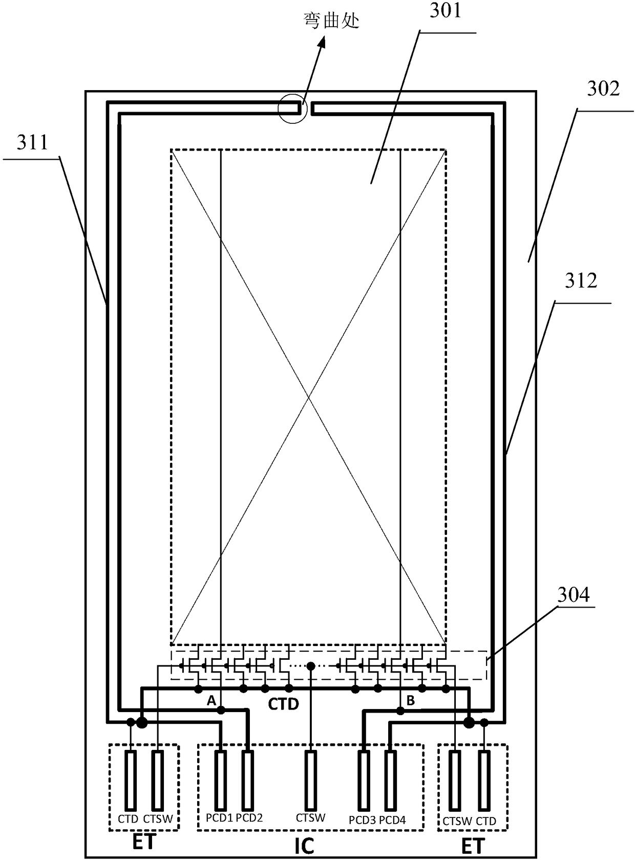
[0052] A structure of a display panel provided by Embodiment 2 of the present invention, such as image 3 As shown, it includes: a display area 301 and a non-display area 302 surrounding the display area. Two metal wires are arranged in the non-display area 302, wherein the first metal line 311 is formed in the non-display area on the left. The inner and outer layers of crack detection wires surrounding the left display area; the second metal wire 312 in the right non-display area forms the inner and outer layers of crack detection wires surrounding the right display area.
[0053] Preferably, if image 3 As shown, the start and end of the first metal wire 311 are located on the same side of the display panel, and the start of the first metal wire 311 is located in the outer layer, that is, the start of the first metal wire 311 is a crack in the outer layer. Detection wires; the bend between the inner and outer layers of crack detection wires formed by the first metal wire is...
Embodiment 3
[0064] A structure of a display panel provided by Embodiment 3 of the present invention, such as Figure 4 As shown, it includes: a display area 401 and a non-display area 402 surrounding the display area. Two metal wires are arranged in the non-display area 402, wherein the first metal line 411 is formed in the non-display area on the left. The inner and outer layers of crack detection wires surrounding the left display area; the second metal wire 412 in the right non-display area forms the inner and outer layers of crack detection wires surrounding the right display area.
[0065] Preferably, if Figure 4 As shown, the start and end of the first metal wire 411 are located on the same side of the display panel, and the start of the first metal wire 411 is located in the outer layer, that is, the start of the first metal wire 411 is a crack in the outer layer. Detection wires; the bend between the inner and outer layers of crack detection wires formed by the first metal wire ...
PUM
 Abstract
Description
Claims
Application Information