A switch power supply device
A switching power supply and switching element technology, applied in the output power conversion device, electrical components, regulating electrical variables and other directions, can solve problems such as the inability to obtain peak power
- Summary
- Abstract
- Description
- Claims
- Application Information
AI Technical Summary
Problems solved by technology
Method used
Image

Examples
Embodiment 1
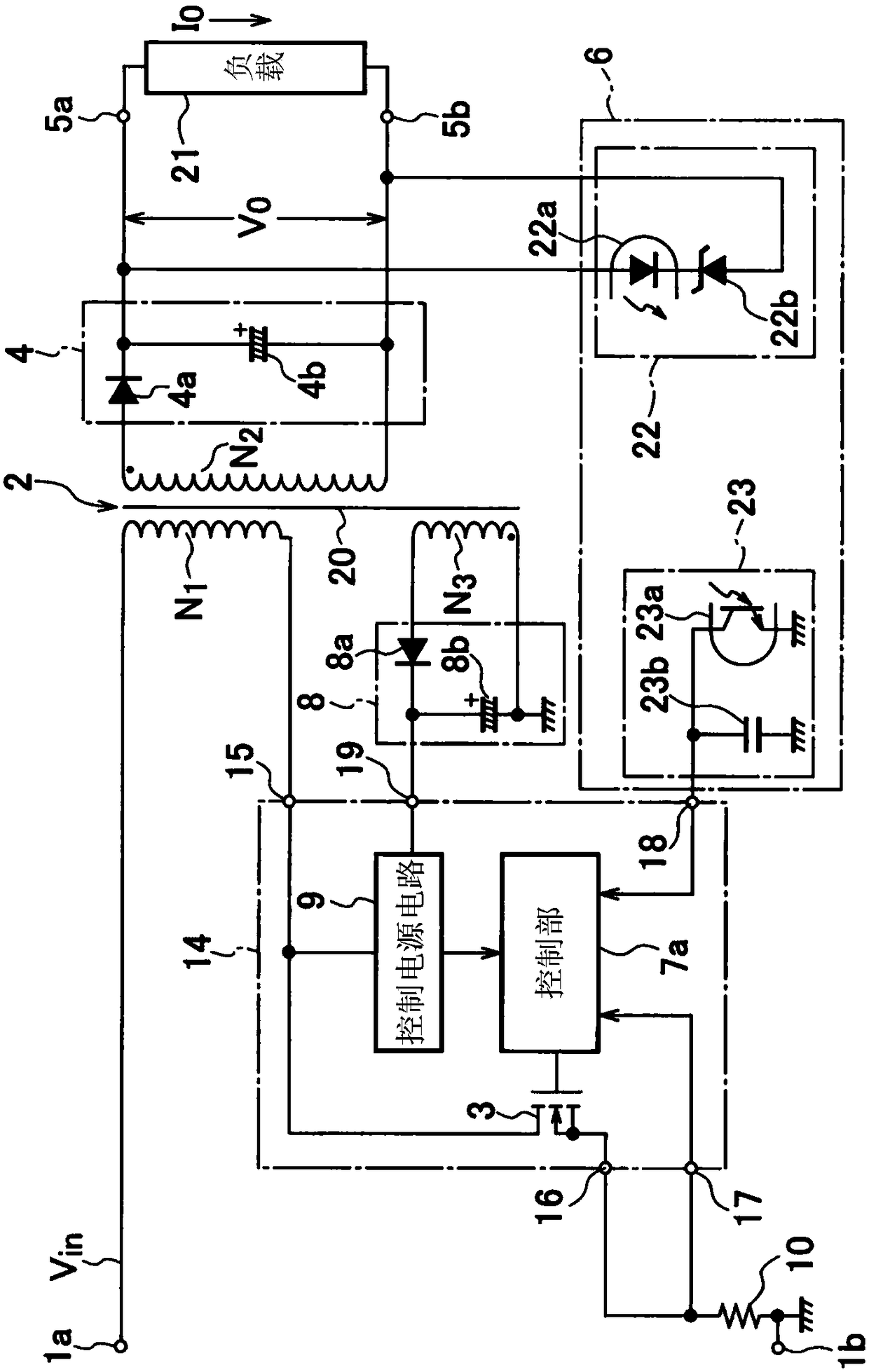
[0040] figure 1 The switching power supply device of the shown embodiment 1 is characterized in that a control section 7a is provided instead of Figure 8 The control part 7 of the conventional switching power supply apparatus shown. exist figure 1 in, right with Figure 8 The same reference numerals are assigned to the same parts, and description thereof will be omitted.
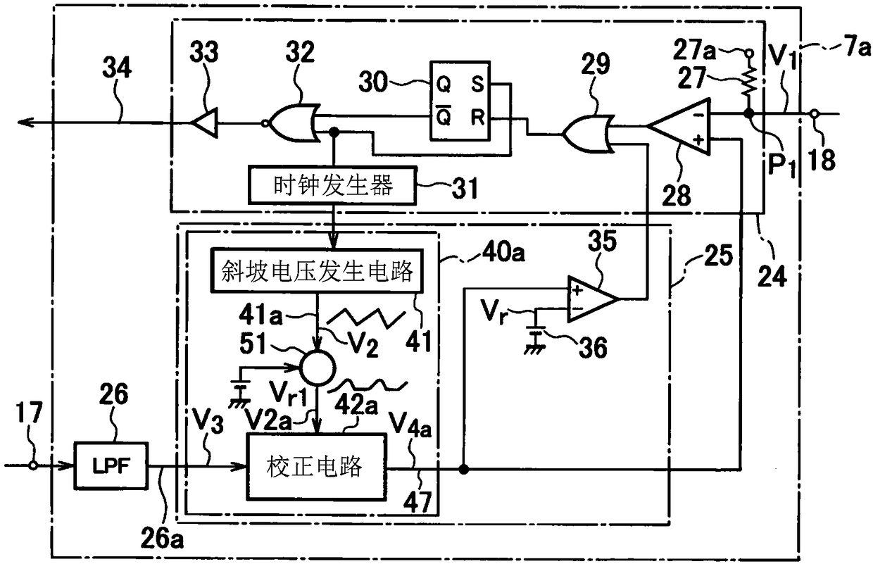
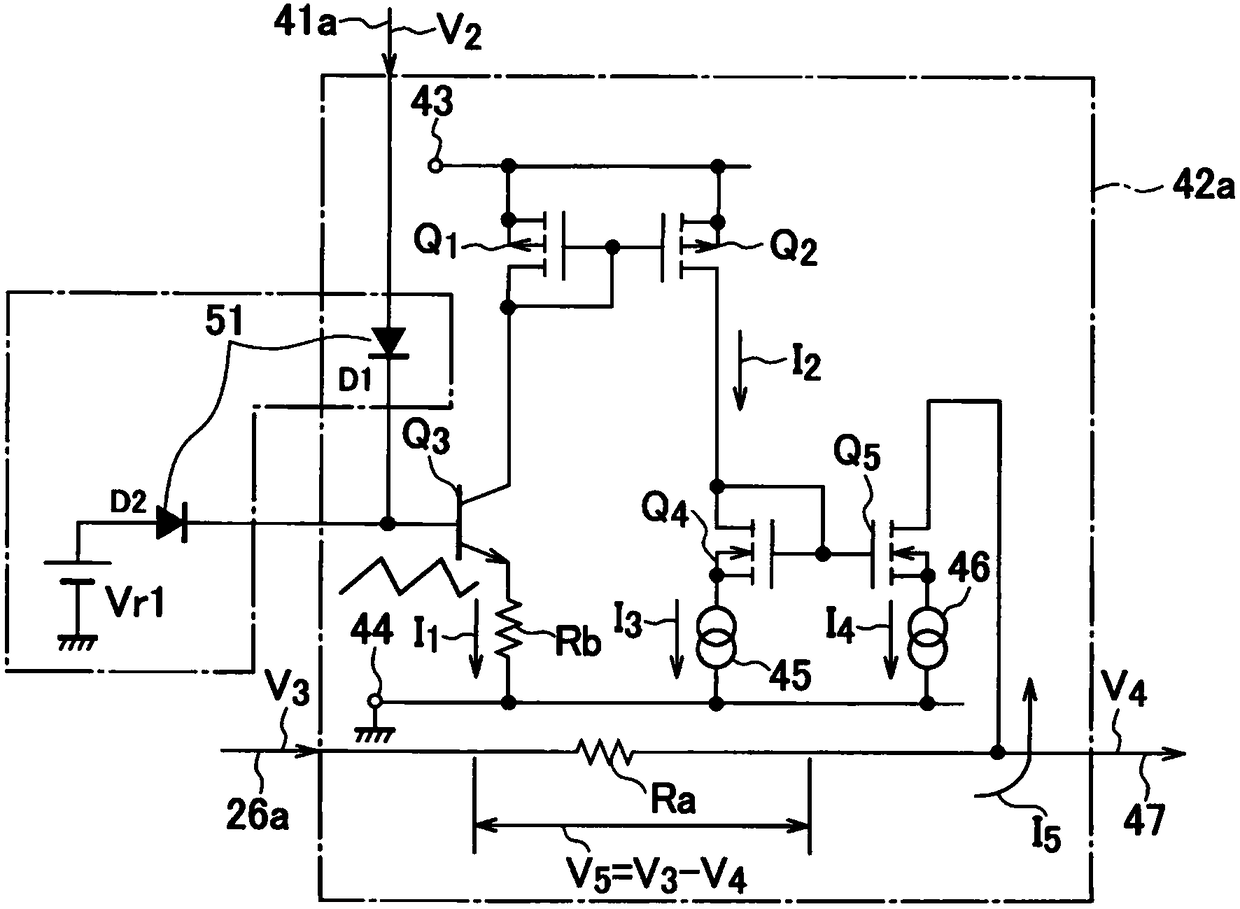
[0041] Such as figure 2 as shown, figure 1 The control section 7a shown with respect to Figure 8 The shown configuration of the conventional control unit 7 differs in the configuration of the correction current detection signal generation unit 40a. The correction current detection signal generation unit 40a has a ramp voltage generation circuit 41, a reference voltage source Vr1, an adder 51, and a correction circuit 42a.
[0042] The correction current detection signal generation unit 40a responds to the signal indicating the timing of the start of the conduction of the switching element 3 in the ...
Embodiment 2
[0056] Figure 5 It is a detailed circuit diagram of the control unit 7b provided in the switching power supply device of the second embodiment. Figure 6 yes Figure 5 A detailed circuit diagram of the adder 51a, the switch SW and the correction circuit 42b is shown. The correction current detection signal generation unit 40b included in the control unit 7b has a ramp voltage generation circuit 41, a reference voltage source Vr1, an adder 51a, a switch SW connected to the reference voltage source Vr1 and the adder 51a, and a correction circuit 42b.
[0057] In addition, the control unit 7b has a duty ratio detection circuit 52 that detects the duty ratio, turns on the switch SW when the duty ratio is smaller than a predetermined value, and turns on the switch SW when the duty ratio is a predetermined value. The switch SW is turned off during the period above the value.
[0058] Specifically, the duty ratio detection circuit 52 is connected to the output terminal of the NOR...
Embodiment 3
[0064] Figure 7 It is a detailed circuit diagram of the control unit 7c provided in the switching power supply device according to the third embodiment of the present invention. The corrected current detection signal generating unit 40c included in the control unit 7c includes a ramp voltage generating circuit 41, a reference voltage source Vr1, an adder 51b, a switch SW connected to the reference voltage source Vr1 and the adder 51b, and a correction circuit 42c.
[0065] The correction current detection signal generating unit 40c responds to the signal indicating the conduction start timing of the switching element 3 in the on / off control signal forming circuit 24, and when the input voltage is lower than a predetermined voltage, generates a signal from the switching element 3 A first correction signal having a constant value is formed during a period in which the duty ratio is smaller than a predetermined value from the conduction start time of , and a time elapsed from th...
PUM
 Abstract
Description
Claims
Application Information
 - R&D
- Intellectual Property
- Life Sciences
- Materials
- Tech Scout
- Unparalleled Data Quality
- Higher Quality Content
- 60% Fewer Hallucinations
Browse by: Latest US Patents, China's latest patents, Technical Efficacy Thesaurus, Application Domain, Technology Topic, Popular Technical Reports.
© 2025 PatSnap. All rights reserved.Legal|Privacy policy|Modern Slavery Act Transparency Statement|Sitemap|About US| Contact US: help@patsnap.com