
Electronic components and display devices

A technology for electronic components and display devices, applied in the direction of identification devices, electrical components, electrical solid devices, etc., can solve the problems of physical connection, unstable electrical connection, inability to transmit signals, and reduced yield, so as to avoid short-circuit or state The effect of bad bonding and improving bonding yield

Active Publication Date: 2020-07-24
KUNSHAN GO VISIONOX OPTO ELECTRONICS CO LTD
View PDF11 Cites 0 Cited by
  • Summary
  • Abstract
  • Description
  • Claims
  • Application Information

AI Technical Summary

Problems solved by technology

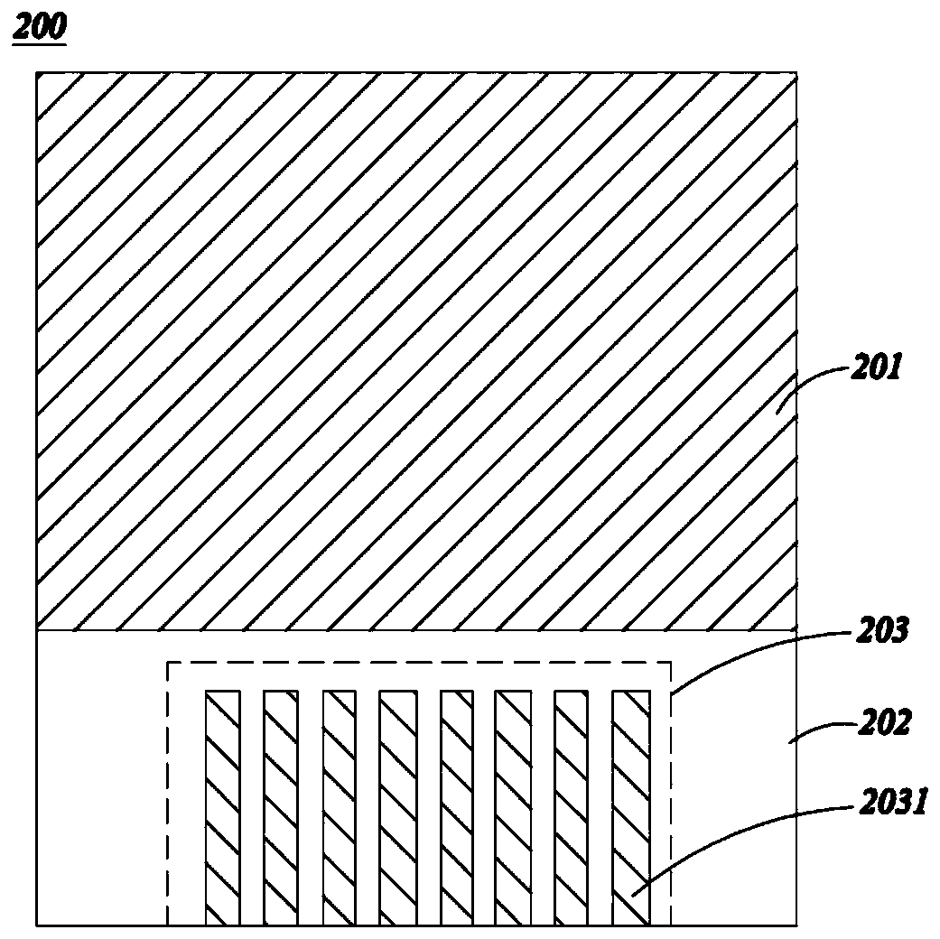
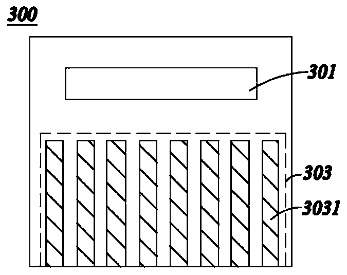
For example, the first pin 2031 is not in contact with the corresponding second pin 3031, so that the signal cannot be transmitted; or, the contact area between the first pin 2031 and the corresponding second pin 3031 is too small, resulting in a physical The connection and electrical connection are unstable; or, one first pin 2031 is connected to two second pins 3031 at the same time, resulting in a short circuit, etc., which reduces the bonding yield

Method used


Image

  • Electronic components and display devices
  • Electronic components and display devices
  • Electronic components and display devices

Examples


Embodiment Construction

[0043] The present invention will be described in detail below in conjunction with specific embodiments shown in the accompanying drawings. However, these embodiments do not limit the present invention, and any structural, method, or functional changes made by those skilled in the art according to these embodiments are included in the protection scope of the present invention.

[0044] In each drawing of the present invention, for convenience of illustration, some dimensions of structures or parts are exaggerated relative to other structures or parts, and therefore, are only used to illustrate the basic structure of the subject matter of the present invention.

[0045]In addition, terms used herein such as "upper", "above", "under", "below", etc. to express relative positions in space are for convenience of description to describe a unit or feature as shown in the drawings relative to A relationship to another cell or feature. The terms of spatial relative position may be int...


PUM


Abstract

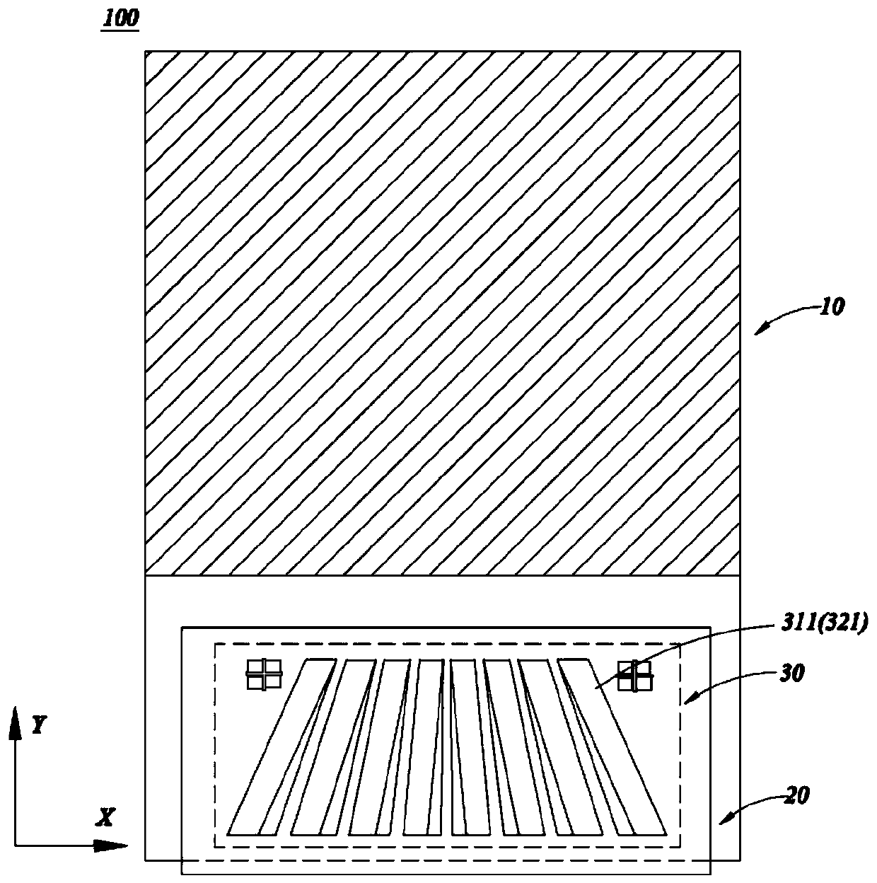
The invention relates to an electronic assembly and a display device; the electronic assembly comprises a first binding zone and a second binding zone mutually matched; the first and second binding zones respectively comprise a plurality of first and second pins arranged at intervals, wherein the first pin has a first end and a second end, and the second pin has a third end and a fourth end; in the arrangement direction of the first pins, a first distance between the most outer sides of two first ends of the two most outer first pins is smaller than a second distance between the most outer sides of the two second ends; a first width ratio is formed between the first and third ends of at least one corresponding first pin and second pin, and a second width ratio is formed between the secondand fourth ends, wherein the first width ratio and the second width ratio are different. The contraposition deviations between the plurality of first and second pins can be effectively rectified; theavailable binding zone is relatively large in area, thus greatly improving the binding yield rate.

Description

technical field [0001] The invention relates to the field of display technology, in particular to an electronic component and a display device. Background technique [0002] Today, with the development of multimedia technology and the advent of the information society, the requirements for electronic equipment are getting higher and higher, such as display equipment, communication equipment and so on. [0003] Taking display equipment as an example, in recent years, three new display technologies have emerged: plasma display, field emission display and organic electroluminescent display, all of which have made up for the shortcomings of cathode ray tubes and liquid crystal displays to a certain extent. [0004] Among them, Organic Light Emitting Devices (OLED) has a series of advantages such as self-luminescence, low-voltage DC drive, full curing, wide viewing angle, and rich colors. Compared with liquid crystal displays, organic light emitting displays No backlight is requ...

Claims


Application Information

Patent Timeline
Patent Type & Authority Patents(China)
IPC IPC(8): H01L23/49G09F9/33
CPCG09F9/33H01L23/49
Inventor 朱晖段培
Owner KUNSHAN GO VISIONOX OPTO ELECTRONICS CO LTD
Learn More