Supercharge Your Innovation With Domain-Expert AI Agents!

Method for manufacturing semiconductor device

A semiconductor and device technology, applied in the field of manufacturing semiconductor devices, can solve problems such as complex and expensive manufacturing of 3D semiconductor storage devices

Pending Publication Date: 2018-09-25
SAMSUNG ELECTRONICS CO LTD
View PDF4 Cites 1 Cited by
  • Summary
  • Abstract
  • Description
  • Claims
  • Application Information

AI Technical Summary

Problems solved by technology

However, 3D semiconductor memory devices can be relatively expensive and more complex to manufacture than 2D semiconductor memory devices.

Method used


Image

  • Method for manufacturing semiconductor device
  • Method for manufacturing semiconductor device
  • Method for manufacturing semiconductor device

Examples


Embodiment Construction

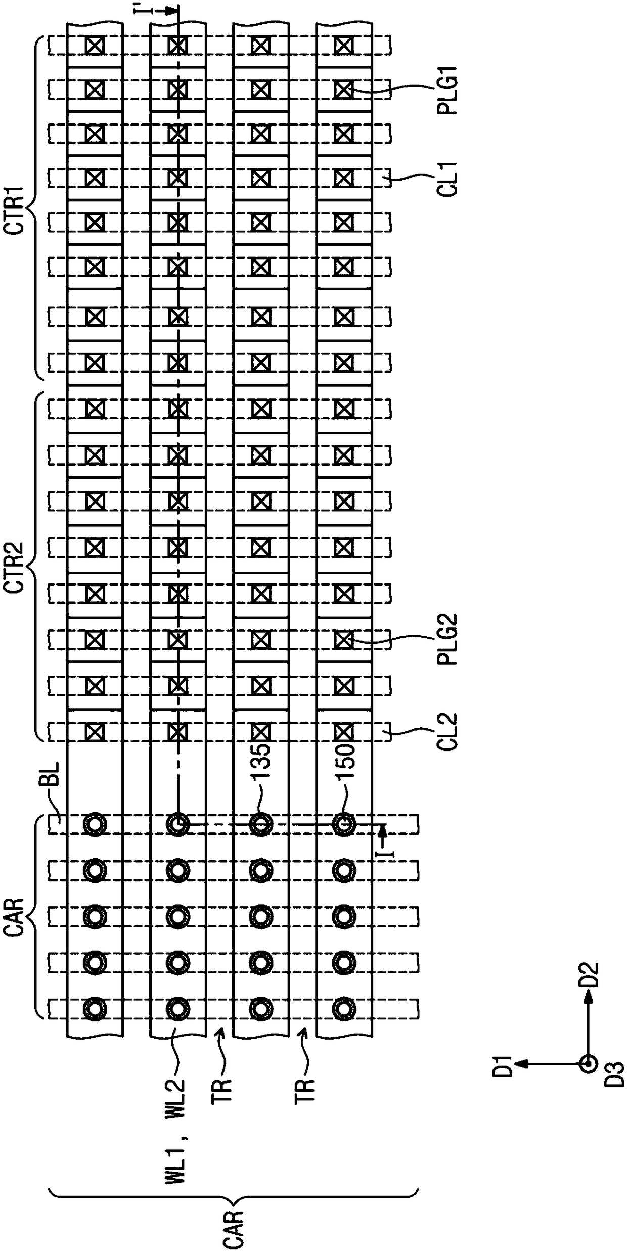
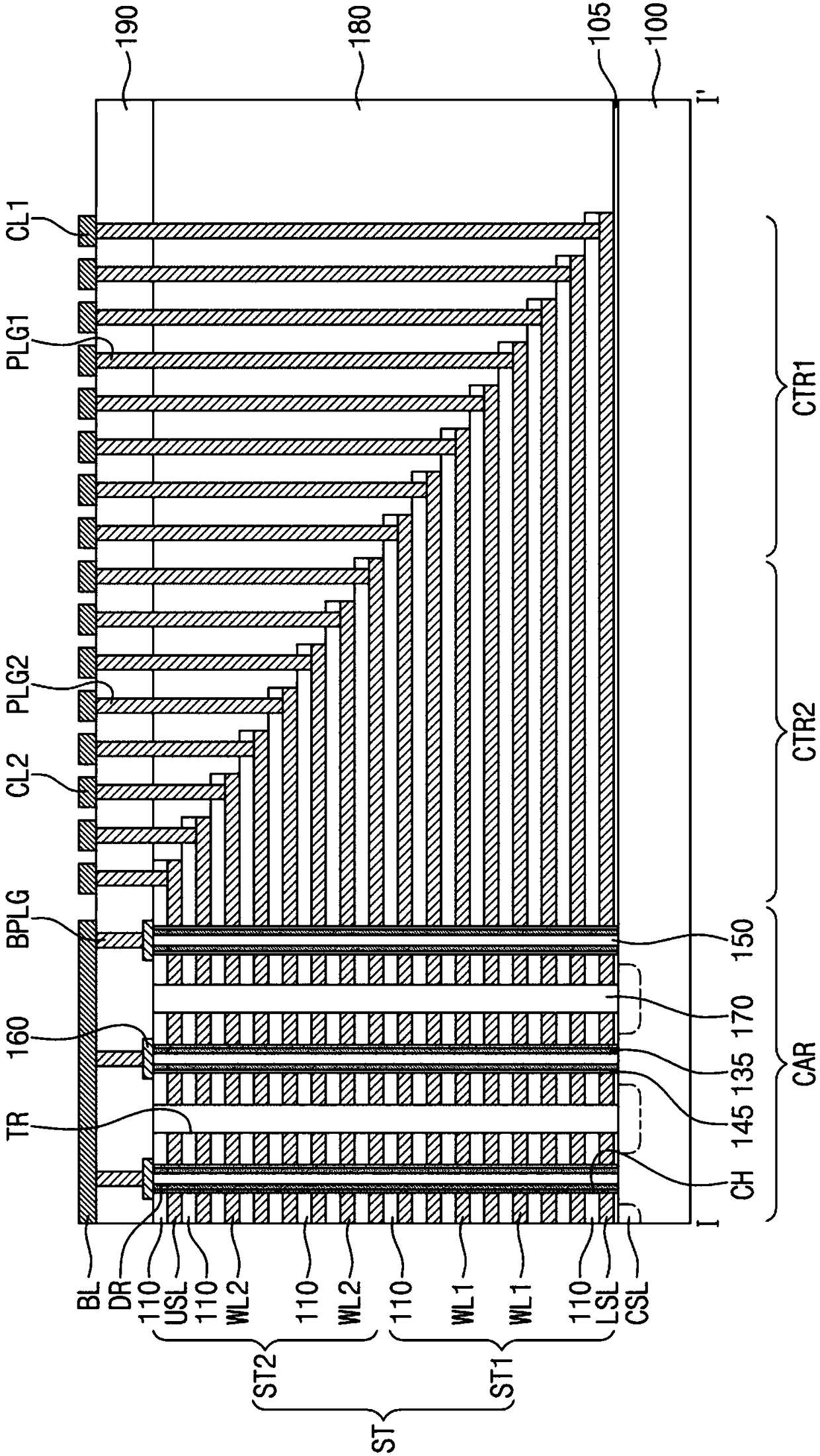
[0052] Exemplary embodiments of the present inventive concept will now be described in more detail with reference to the accompanying drawings, in which exemplary embodiments are shown. However, exemplary embodiments of the inventive concept may be embodied in many different forms, and should not be construed as limited to the exemplary embodiments set forth herein. In the drawings, exemplary embodiments of the inventive concepts are not limited to specific examples provided herein, and components, layers, or regions shown in the drawings may be exaggerated for clarity of description.

[0053] In the specification and drawings, it will be understood that when an element such as a layer, region or substrate is referred to as being “on” another element, it can be directly on the other element or intervening elements may be present. Throughout the specification and drawings, the same reference numerals or the same figure designators may denote the same elements.

[0054] Exempla...


PUM


Abstract

The scheme of the invention provides a method for manufacturing a semiconductor device. The method comprises the steps: alternately and repeatedly stacking insulating layers and sacrificial layers ona substrate to form a stacked structure; sequentially forming a first lower layer and a first photoresist pattern on the stacked structure; employing the first photoresist pattern as an etching mask for etching the first lower layer to form a first lower pattern; employing the first lower pattern as an etching mask for etching a first part of the stacked structure to form a stepped structure. Thefirst lower layer includes a novolak-based organic polymer, and the first photoresist pattern includes a silicon-containing polymer.

Description

technical field [0001] Exemplary embodiments of the inventive concepts relate to semiconductor devices, and more particularly, to methods for manufacturing semiconductor devices. Background technique [0002] Semiconductor devices have been highly integrated and can provide high performance and low cost. The integration density of a semiconductor device can affect the cost of the semiconductor device. The integration density of a two-dimensional (2D) or planar memory device may be mainly determined by the area occupied by a unit memory cell. Therefore, the integration density of a 2D memory device may be affected by a technique for forming fine patterns. However, the manufacturing capability of relatively high-density 2D memory devices may be limited because relatively high-priced equipment may be used to form fine patterns. [0003] Three-dimensional (3D) semiconductor devices including memory cells arranged three-dimensionally have been developed to increase integration...

Claims


Application Information

Patent Timeline
IPC IPC(8): H01L21/027
CPCH01L21/0274H10B41/20
Inventor 洪锡九姜美荣李孝圣赵庆容金宝螺金惠智赵先觉
Owner SAMSUNG ELECTRONICS CO LTD
Features
  • R&D
  • Intellectual Property
  • Life Sciences
  • Materials
  • Tech Scout
  • Unparalleled Data Quality
  • Higher Quality Content
  • 60% Fewer Hallucinations
Learn More