Supercharge Your Innovation With Domain-Expert AI Agents!

Array substrate

An array substrate and array technology, applied in nonlinear optics, instruments, optics, etc., can solve the problem that the longitudinal length of the external lead area cannot be effectively reduced, the space of the external lead area cannot be effectively used, and the narrow frame and other issues to achieve the effect of reducing the vertical length

Pending Publication Date: 2018-10-02
AU OPTRONICS CORP
View PDF8 Cites 1 Cited by
  • Summary
  • Abstract
  • Description
  • Claims
  • Application Information

AI Technical Summary

Problems solved by technology

However, the current connection method between the driving circuit and the connection pads of the external pin area does not effectively utilize the space of the external pin area, so that the vertical length of the external pin area cannot be effectively reduced
As a result, the goal of narrow borders has not been fully realized

Method used


Image

  • Array substrate
  • Array substrate
  • Array substrate

Examples


Embodiment Construction

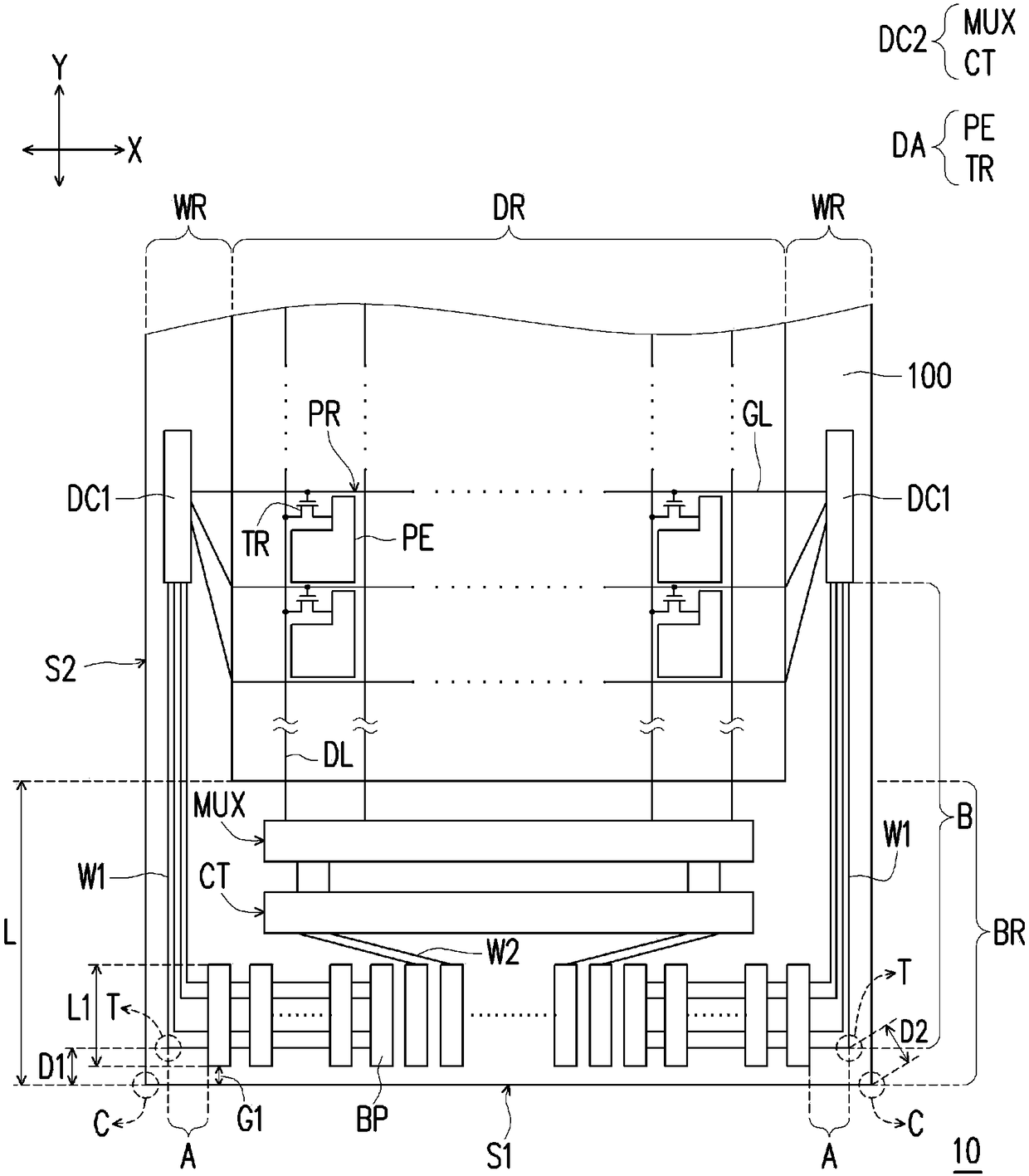
[0057] figure 1 is a schematic top view of the array substrate 10 according to an embodiment of the present invention.

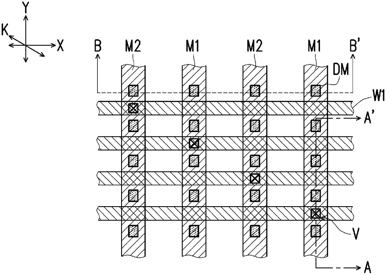
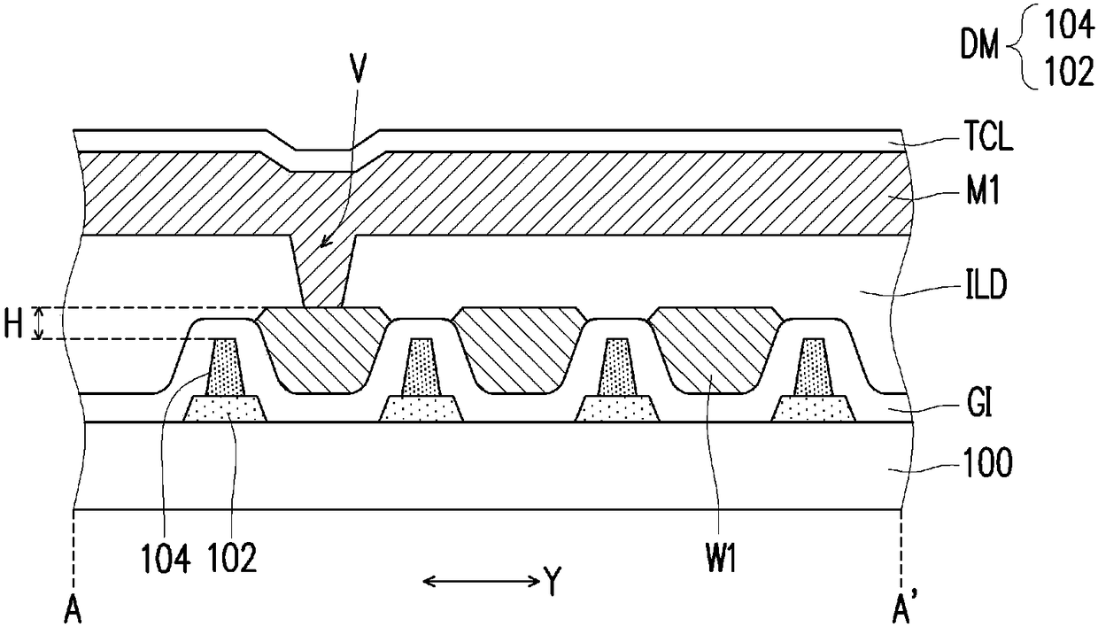
[0058] Please refer to figure 1 , the array substrate 10 of the embodiment of the present invention includes a base 100 . In some embodiments, the substrate 100 is a transparent substrate. For example, the material of the substrate 100 may include glass. In this embodiment, the substrate 100 has a first side S1 and a second side S2 adjacent to each other. The first side S1 extends along the first direction X, and the second side S2 extends along the second direction Y. The first direction X and the second direction Y intersect. In some embodiments, the first direction X is perpendicular to the second direction Y. The substrate 100 has a display area DR, a wiring area WR and an outer lead bond area BR. The display region DR has a plurality of pixel regions PR. The plurality of pixel regions PR are arranged in an array along the first direction X and t...


PUM

PropertyMeasurementUnit
widthaaaaaaaaaa

Abstract

An array substrate includes a substrate, an element array, a driving circuit, a plurality of connection pads, and a plurality of connection lines. The element array, the driving circuit, the pluralityof connection pads, and the plurality of connection lines are formed on the substrate. The driving circuit is electrically connected to the component array. A plurality of connection pads are arranged substantially along a first side of the substrate. A plurality of connecting wires are electrically connected between the driving circuit and the plurality of connecting pads. Each connecting line has a turning portion. The distance between the outermost turning portion and the first side is D1. The outermost connecting pad has a length L1. The distance between the outermost connecting pad and the first side is G1, and L1+G1>=D1.

Description

technical field [0001] The present invention relates to an array substrate, and in particular to an array substrate of a display device. Background technique [0002] In recent years, display devices continue to develop toward high resolution and narrow borders. Generally speaking, an array substrate of a display device includes a display area and an outer lead bond area and a wiring area surrounding the display area. The wiring area has a driving circuit, which is used to drive active elements in the display area. However, the current connection method between the driving circuit and the connection pads of the external lead area cannot effectively utilize the space of the external lead area, so that the vertical length of the external lead area cannot be effectively reduced. As a result, the goal of narrow borders has not been fully realized. Contents of the invention [0003] An array substrate according to an embodiment of the present invention includes a substrate, ...

Claims


Application Information

Patent Timeline
Patent Type & Authority Applications(China)
IPC IPC(8): G02F1/1345
CPCG02F1/13452
Inventor 黄士杰吕旻洲
Owner AU OPTRONICS CORP
Features
  • R&D
  • Intellectual Property
  • Life Sciences
  • Materials
  • Tech Scout
  • Unparalleled Data Quality
  • Higher Quality Content
  • 60% Fewer Hallucinations
Learn More