Method for eliminating mutual interference between multiple pairs of dual array elements in single-antenna full-duplex communication

A single-antenna, mutual interference technology, applied in the field of communication, can solve problems such as inappropriate large-scale communication

Inactive Publication Date: 2018-10-02
XIDIAN UNIV
4 Cites 0 Cited by

AI-Extracted Technical Summary

Problems solved by technology

[0012] In addition, the above three technologies also have a common feature, that is, they are not suita...

Abstract

The invention discloses a method for eliminating mutual interference between multiple pairs of dual array elements in single-antenna full-duplex communication. According to the overall idea of the invention, the basic unit of multi-array element mutual interference cancellation is studied based on a mutual interference cancellation principle, and an equivalent baseband model for a single-antenna multi-pair dual-array element primary radio frequency channel is established; and positive and negative array element distribution is designed based on a fractal model with a single pair of dual arrayelements as the basic unit, so that fractal array elements that can multi-dimensionally cancel multi-array element mutual interference is formed. According to the method of the invention, a transmitting antenna and a receiving antenna share one antenna, and therefore, part of the antenna and bandwidth resources can be saved; ad mutual interference in simultaneous co-frequency full-duplex communication can be effectively eliminated under the premise that antenna resources are not wasted, and therefore, the spectrum efficiency of the communication can be effectively improved, and spectrum efficiency is higher. The method is suitable for large-scale communication situations.

Application Domain

Duplex signal operation

Technology Topic

Radio frequencyFrequency spectrum +3

Image

  • Method for eliminating mutual interference between multiple pairs of dual array elements in single-antenna full-duplex communication
  • Method for eliminating mutual interference between multiple pairs of dual array elements in single-antenna full-duplex communication
  • Method for eliminating mutual interference between multiple pairs of dual array elements in single-antenna full-duplex communication

Examples

  • Experimental program(1)

Example Embodiment

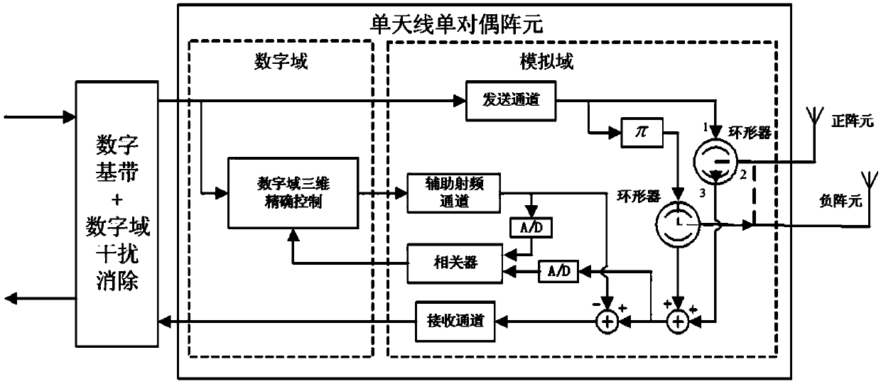
[0103] In the method for eliminating mutual interference between multi-dual array elements in single-antenna full-duplex communication provided by the present invention, single-antenna multi-dual array elements refer to a common antenna for transmitting and receiving, and a number of dual array elements are configured in it, and each dual The array element is composed of a positive array element and a negative array element. The positive array element and the negative array element emit the same signal, and the phase difference between the two is 180 degrees.
[0104] The overall idea of ​​the method for eliminating mutual interference between multi-pair array elements in single-antenna full-duplex communication of the present invention is as follows:
[0105] First of all, based on the principle of mutual interference cancellation, the basic unit of mutual interference cancellation of multiple array elements is studied, that is, the hybrid structure of single-array element self-interference cancellation and dual-array element mutual interference cancellation;
[0106] Then, based on the fractal model with the single dual array element as the basic unit, the positive and negative array element distribution is designed to form a fractal array element that can cancel the mutual interference of multiple array elements in multiple dimensions.
[0107] In the present invention, we use rectangular fractals. Hereinafter, the present invention will be specifically introduced with reference to the drawings and specific embodiments.
[0108] The method provided by the present invention for eliminating mutual interference between multi-pair array elements in single-antenna simultaneous same-frequency full-duplex communication specifically includes the following steps:
[0109] 1. Establish an equivalent baseband model for the main RF channel of single antenna multi-dual array element
[0110] First, we first establish the equivalent baseband model of the main RF channel (signal channel) in the case of a single dual array element, and then derive the equivalent baseband model of the main RF channel of the multi-dual array element.
[0111] In the method provided by the present invention, the single-antenna single-dual array element refers to a common antenna for transmitting and receiving, and a positive array element and a negative array element are configured in it. The positive and negative elements emit the same signal, and the phase difference between the two is 180. degree.
[0112] figure 1 It is a system block diagram of the single antenna single dual array element of the present invention.
[0113] In the case of a single dual array element, the equivalent baseband model of the main RF channel of the single dual array element is shown in the following formula:
[0114]
[0115] among them:
[0116] I p (t) represents the impulse response of the main RF channel of the positive array element;
[0117] I n (t) represents the impulse response of the main RF channel of the negative array element;
[0118] L represents the number of multipaths in the multipath channel;
[0119] a l (t) represents the amplitude response of the first path;
[0120] θ l (t) represents the phase shift of the first path;
[0121] τ l Indicates the delay of the first path;
[0122] δ(t-τ l ) Means the time delay is τ l Shock function at time;
[0123] j represents the unit of imaginary number;
[0124] When the local positive and negative array elements are respectively connected to a circulator, it is equivalent to accessing a new channel. The equivalent baseband model for the main RF channel of the positive and negative array elements and the channel of the circulator are combined. Product, the new expression of the channel of the circulator is obtained, as follows:
[0125]
[0126] among them:
[0127] * Indicates convolution;
[0128] ε ab Indicates the time delay from port a to port b of the circulator of the positive element (ab∈{12,13,23});
[0129] Indicates the delay from port a to port b of the circulator of the negative element (ab∈{12,13,23});
[0130] k ab (t-ε ab ) Represents the amplitude response from port a to port b of the circulator of the positive element (ab∈{12,13,23});
[0131] Represents the amplitude response from port a to port b of the circulator of the negative element (ab∈{12,13,23});
[0132] ω ab (t-ε ab ) Represents the phase shift from port a to port b of the circulator of the positive element (ab∈{12,13,23});
[0133] Indicates the phase shift from port a to port b of the circulator of the negative element (ab∈{12,13,23});
[0134] h n,p (t-η n,p ) Represents the impulse response of the wireless channel from the circulator of the negative element to the circulator of the positive element, η n,p Is its delay;
[0135] h p,n (t-η p,n ) Represents the impulse response of the wireless channel from the circulator of the positive element to the circulator of the negative element, η p,n Is its time delay.
[0136] Then, based on the equivalent baseband model of the single-dual array element, the equivalent baseband model for the main RF channel of the single-antenna multi-dual array element is established. Taking the i-th dual array element as a reference, the formula of the equivalent baseband model is specific as follows:
[0137]
[0138] among them:
[0139] I i,p (t) represents the impulse response of the main RF channel of the positive array element in the i-th dual array element;
[0140] I i,n (t) represents the impulse response of the main RF channel of the negative array element in the i-th dual array element;
[0141] The formula represents the impulse response of the self-interference channel of the positive array element in the i-th dual array element;
[0142] The formula represents the impulse response of the mutual interference channel between the positive array element and the other I-1 positive array elements in the i-th dual array element;
[0143] The formula represents the impulse response of the mutual interference channel between the positive array element and the other I negative array elements in the i-th dual array element;
[0144] The formula represents the impulse response of the self-interference channel of the negative array element in the i-th dual array element;
[0145] The formula represents the impulse response of the mutual interference channel between the negative array element and the other I-1 negative array elements in the i-th dual array element;
[0146] The formula represents the impulse response of the mutual interference channel between the negative array element and the other I positive array elements in the i-th dual array element;
[0147] ε i,ab Represents the delay from port a to port b of the circulator of the i-th positive element (ab∈{12,13,23});
[0148] Represents the delay from port a to port b of the circulator of the i-th negative element (ab∈{12,13,23});
[0149] ε j,ab Represents the delay from port a to port b of the circulator of the j-th positive element (ab∈{12,13,23});
[0150] Represents the time delay from port a to port b of the circulator of the jth negative element (ab∈{12,13,23});
[0151] a l (t-τ l ) Represents the amplitude response of the first path;
[0152] θ l (t-τ l ) Represents the phase shift of the first path;
[0153] k i,ab (t-ε i,ab ) Represents the amplitude response from port a to port b of the circulator of the i-th positive element (ab∈{12,13,23});
[0154] Represents the amplitude response from port a to port b of the circulator of the i-th negative element (ab∈{12,13,23});
[0155] k j,ab (t-ε j,ab ) Represents the amplitude response from port a to port b of the circulator of the j-th positive element (ab∈{12,13,23});
[0156] Represents the amplitude response from port a to port b of the circulator of the jth negative element (ab∈{12,13,23});
[0157] ω i,ab (t-ε i,ab ) Represents the phase shift from port a to port b of the circulator of the i-th positive element;
[0158] Represents the phase shift from port a to port b of the circulator of the i-th negative element;
[0159] ω j,ab (t-ε j,ab ) Represents the phase shift from port a to port b of the circulator of the j-th positive element;
[0160] Indicates the phase shift from port a to port b of the circulator of the jth negative element;
[0161] h jp,ip (t-η jp,ip ) Represents the impulse response of the wireless channel from the circulator of the j-th positive element to the circulator of the i-th positive element, η jp,ip Is its delay;
[0162] h jn,ip (t-η jn,ip ) Represents the impulse response of the wireless channel from the circulator of the j-th negative element to the circulator of the i-th positive element, η jn,ip Is its delay;
[0163] h jn,in (t-η jn,in ) Represents the impulse response of the wireless channel from the circulator of the j-th negative element to the circulator of the i-th negative element, η jn,in Is its delay;
[0164] h jp,in (t-η jp,in ) Represents the impulse response of the wireless channel from the circulator of the j-th positive element to the circulator of the i-th negative element, η jp,in Is its time delay.
[0165] 2. Design fractal structure
[0166] For the case of a single antenna with multiple dual array elements, we have placed I dual array elements on the rectangular fractal geometry.
[0167] figure 2 It is a schematic diagram of the rectangular fractal structure of the single antenna multi-dual array element of the present invention.
[0168] Under ideal circumstances, the positive and negative elements in a dual element can ensure good orthogonality (the distance between the positive and negative elements is ), and the mutual interference between different dual array elements is zero.
[0169] To facilitate understanding, we use Represents the output signal of multiple dual array elements after fractal interference cancellation in the case of single antenna and multiple dual array elements, The expression is as follows:
[0170]
[0171] among them:
[0172] y u (t) represents the useful signal, x(t) represents the locally known interference signal, γ i (t) represents the channel impulse response from port 2 to port 3 of the circulator of positive and negative elements in the i dual array elements, a l (t-τ l ) The above formula has been given, θ l (t-τ l ) The above formula has been given;
[0173] Indicates the self-interference impulse response of the main RF channel of the i-th dual array element;
[0174] (If and only if i=j), it means the mutual interference impulse response of the main RF channel of the i-th dual array element;
[0175] Represents the mutual interference impulse response between the j-th positive (negative) element and the i-th positive (negative) element of the same pole (both positive or negative);
[0176] Represents the impulse response of different pole mutual interference between the j-th positive (negative) element and the i-th negative (positive) element;
[0177] μ represents the fractal coefficient.
[0178] Through the analysis of the above formula, we know that the fractal structure mainly cancels the mutual interference between different dual array elements, so we need to require a suitable non-negative number μ to prove that the fractal structure can cancel the mutual interference between different dual array elements under the allowable error. interference.
[0179] According to the above description, we know that when the dual array elements are uniformly distributed on the rectangular fractal, the mutual interference between the dual array elements cancels each other out, and μ=0 at this time.
[0180] Below we analyze the uneven distribution of the dual array elements on the rectangular fractal.
[0181] The interference power we allocate to each element is P T , Then the received mutual interference power P of the i-th dual array element can be obtained i,r for:
[0182]
[0183] among them:
[0184] Represents the distance from the j-th positive (negative) element to the i-th positive (negative) element.
[0185] In the rectangular fractal structure, because there is as well as Relationship, so the mutual interference power between single-antenna multi-dual array elements P r for:
[0186]
[0187] According to the above formula, it can be seen that the rectangular fractal structure can offset the mutual interference between different pairs of array elements.
[0188] therefore, It can be written in the following form:
[0189]
[0190] Considering that the fractal coefficient is non-negative, the fractal coefficient μ can be expressed as:
[0191]
[0192] It can be seen from the μ expression: when satisfied Under the conditions, the mutual interference between different dual array elements can theoretically be offset.
[0193] In this embodiment, we set the power of the mutual interference signal from other dual array elements to be close to 60dB. We can offset the mutual interference between different pairs of array elements through the rectangular fractal structure, so the rectangular fractal structure makes The same pole mutual interference of other dual array elements, the simulation results are as follows image 3 Shown.
[0194] by image 3 It can be seen that after fractal cancellation processing, the power of the mutual interference signal from other dual array elements will decrease with the decrease of μ. In the case of close to uniform fractal geometry (μ=0), the mutual interference signal will be at the corresponding frequency The position will form a deep zero.
[0195] It should be noted that the foregoing embodiments do not limit the present invention in any form, and all technical solutions obtained by equivalent substitutions or equivalent transformations fall within the protection scope of the present invention.

PUM

no PUM

Description & Claims & Application Information

We can also present the details of the Description, Claims and Application information to help users get a comprehensive understanding of the technical details of the patent, such as background art, summary of invention, brief description of drawings, description of embodiments, and other original content. On the other hand, users can also determine the specific scope of protection of the technology through the list of claims; as well as understand the changes in the life cycle of the technology with the presentation of the patent timeline. Login to view more.
Why Eureka
Try Eureka