Method for reducing welding bubble rate of QFN chip and steel mesh structure obtained by applying method

A technology of chip welding and air bubble rate, which is applied in the direction of welding equipment, welding equipment, tin feeding device, etc., can solve the problems affecting the reliability of solder joints, function failure, etc., and achieve simple structure, reduce air bubble rate, and better use effect Effect

Active Publication Date: 2018-10-12
SHANGHAI VEI SHENG AUTO PARTS MFG CO LTD
View PDF5 Cites 2 Cited by
  • Summary
  • Abstract
  • Description
  • Claims
  • Application Information

AI Technical Summary

Problems solved by technology

[0004] However, air bubbles during soldering are a common phenomenon in solder joints. Once there are too many air bubbles, the reliability of solder joints will be seriously affected. According to current statistics, PCBA (PCBA is the abbreviation of Printed Circuit Board+Assembly) is due to the failure of solder joint air bubbles. , that is to say, the PCB empty board passes through the SMT upper part, and then through the entire process of the DIP plug-in) the function fails by 20%

Method used


Image

  • Method for reducing welding bubble rate of QFN chip and steel mesh structure obtained by applying method
  • Method for reducing welding bubble rate of QFN chip and steel mesh structure obtained by applying method
  • Method for reducing welding bubble rate of QFN chip and steel mesh structure obtained by applying method

Examples


Embodiment Construction

[0053] In order to more clearly illustrate the embodiments of the present invention or the technical solutions in the prior art, the specific implementation manners of the present invention will be described below with reference to the accompanying drawings. Apparently, the drawings in the following description are only some embodiments of the present invention, and those skilled in the art can also obtain other implementation manners according to these drawings without creative efforts.

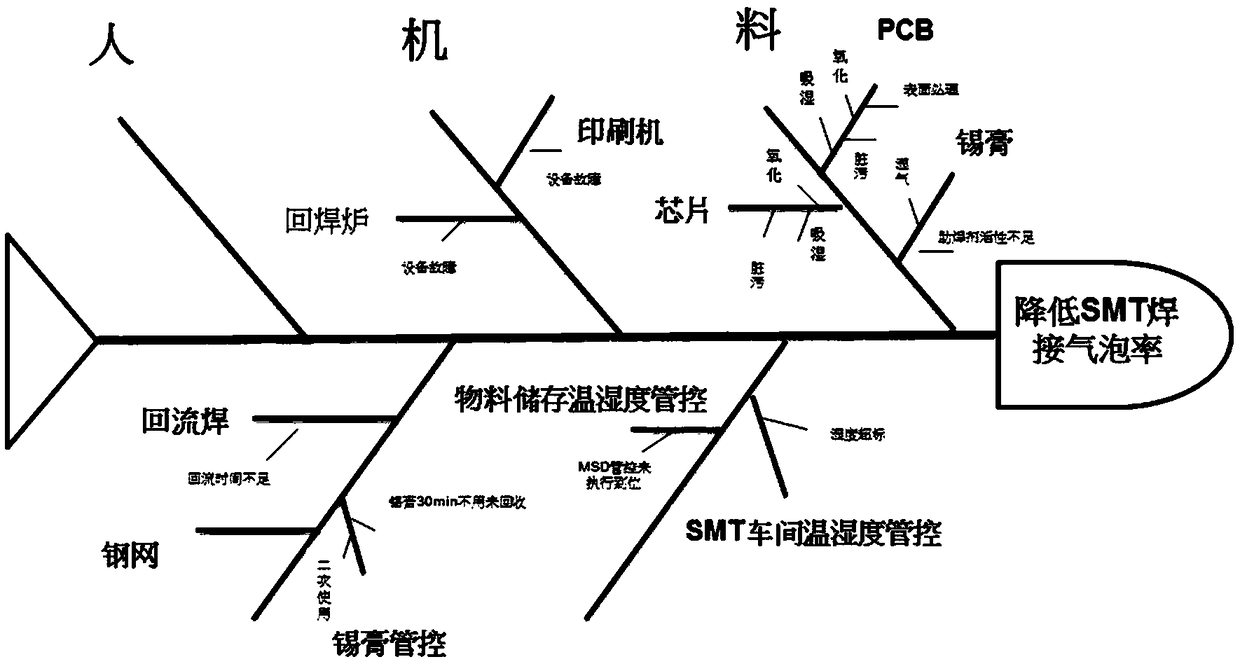
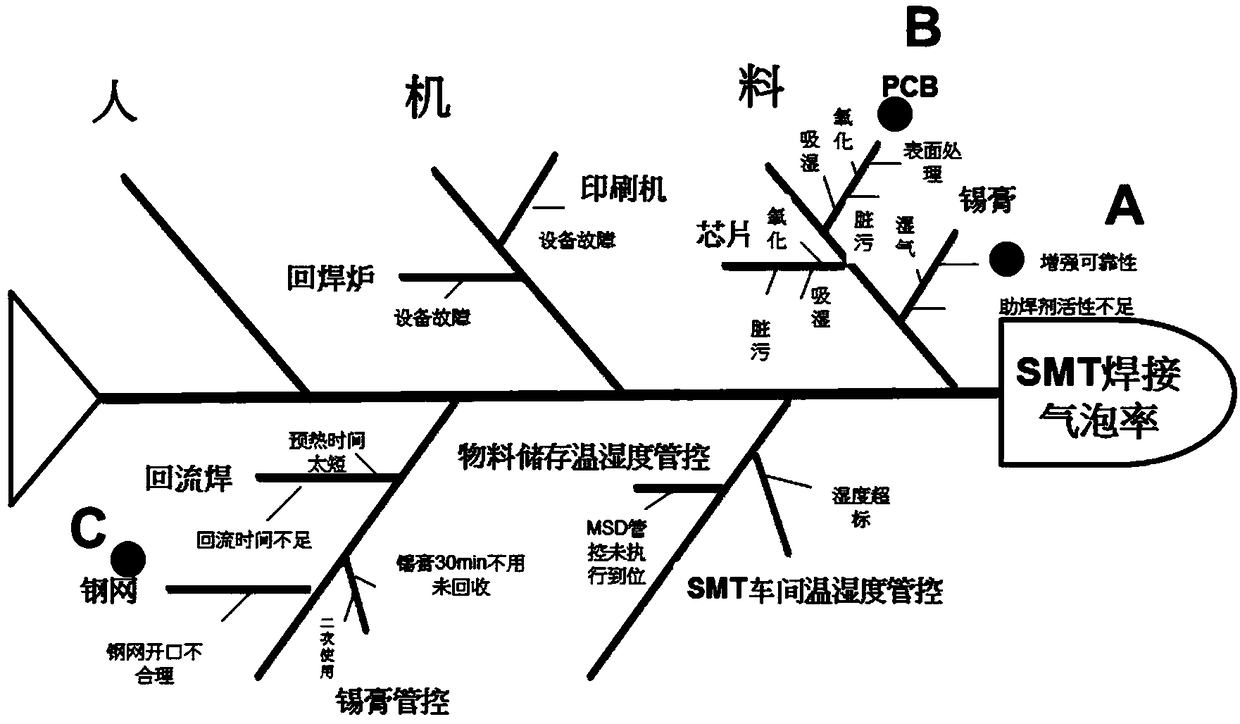
[0054]In an embodiment of the invention, a method for reducing the bubble rate of QFN chip soldering comprises the following steps:

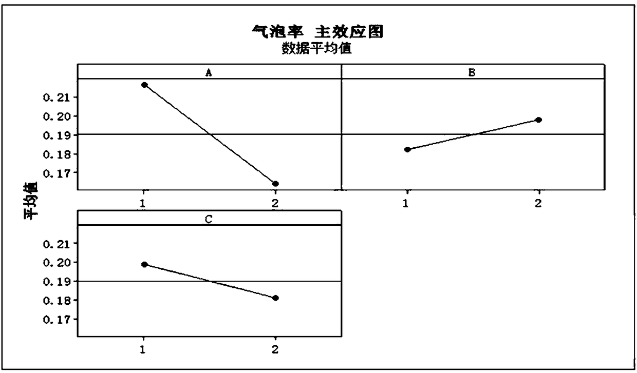
[0055] S01: judge the factors that generate the bubble rate, and obtain the most important factors;

[0056] S02: According to several factors, each factor gives two different first fixed data respectively;

[0057] S03: Each factor in several factors selects a first fixed data respectively, forms the first test group, obtains the bubble rate value of corresp...


PUM


Abstract

The invention relates to a method for reducing a welding bubble rate of a QFN chip and a steel mesh structure obtained by applying the method. The method comprises the following steps of: judging factors of generating a bubble rate to obtain several main factors; separately giving out two different first fixed data by each factor; separately selecting a first fixed datum by each factor in the several factors to define a first test group, thereby obtaining a bubble rate value of the corresponding first test group; obtaining important factors which affect the bubble rate according to the bubblerate value; separately giving out multiple different second fixed data by each important factor according to the important factors; separately selecting a second fixed datum by each important factor to form a second test group to obtain a final bubble rate value of the corresponding second test group; and obtaining final factors which affect the bubble rate value according to the final bubble ratevalue. On the basis of ensuring reliability of a welding spot by the method, the shape of the steel mesh is improved, so that tin amount is increased, and therefore, the bubble rate generated duringwelding is effectively reduced.

Description

technical field [0001] The invention belongs to a device used in semiconductor packaging technology, and in particular relates to a method for reducing the air bubble rate generated during welding during QFN packaging, and a steel mesh structure obtained by the method. Background technique [0002] QFN (Quad Flat No-leadPackage, square flat no-lead package), one of the surface mount packages. It is now mostly called LCC. QFN is a name stipulated by the Japan Electron Machinery Industry Association. There are electrode contacts on the four sides of the package. Since there are no leads, the mounting area is smaller than that of QFP, and the height is lower than that of QFP. However, when stress occurs between the printed substrate and the package, it cannot be relieved at the electrode contact. Therefore, it is difficult to make electrode contacts as many as QFP pins, generally from about 14 to 100. [0003] Because the QFN package does not have gull-wing leads like the t...

Claims


Application Information

Patent Timeline
Patent Type & Authority Applications(China)
IPC IPC(8): B23K31/12B23K3/06B23K101/40
CPCB23K3/0623B23K3/0638B23K31/12
Inventor 林东峰郭振华赵玉琳王立康陈亚姚亚蓉
Owner SHANGHAI VEI SHENG AUTO PARTS MFG CO LTD
Why Eureka
Try Eureka