
A size-adjustable bulk chip component mounting tray

A size and chip technology, which is applied in the field of size-adjustable bulk chip component mounting trays, can solve problems such as difficulty in unifying the thickness direction, increasing time cycle costs, and bulk materials that cannot meet the mounting requirements of the chip mounter.

Active Publication Date: 2019-12-27
CHANGCHUN INST OF OPTICS FINE MECHANICS & PHYSICS CHINESE ACAD OF SCI
View PDF8 Cites 0 Cited by
  • Summary
  • Abstract
  • Description
  • Claims
  • Application Information

AI Technical Summary

Problems solved by technology

[0003] Components of electronic products usually need to be screened before installation. During this process, the tapes that could have been used for mounting will be destroyed, resulting in the screening of bulk materials that cannot meet the mounting requirements of the placement machine. Greatly affected the development of automatic placement equipment performance
At present, although the problem of bulk material machine placement can be solved by re-taping of components, it is difficult to unify the dimensions and specifications of components produced by different manufacturers, especially chip components.
Internationally, surface mount chip package components are clearly defined in the two-dimensional direction, but it is difficult to unify the thickness direction. In order to ensure the quality of the tape, for the same package but different thickness components, all need to be molded and customized The corresponding carrier tape needs to increase the time cycle cost, and the economic cost of mold opening and customization also increases accordingly.

Method used


Image

  • A size-adjustable bulk chip component mounting tray
  • A size-adjustable bulk chip component mounting tray
  • A size-adjustable bulk chip component mounting tray

Examples


Embodiment Construction

[0025] In order to make the practical purpose, technical implementation plan, and solution advantages of the patent of the present invention more clear, the specific implementation of the patent will be detailed below according to the drawings of the patent of invention. In the drawings, the described embodiments are some, not all, embodiments of the present invention. The embodiments described in the drawings are exemplary and are intended to explain the present invention, but should not be construed as limiting the present invention. Based on this embodiment, all other embodiments obtained by persons of ordinary skill in the art without creative efforts fall within the protection scope of the present invention. The present embodiment will be described in detail below in conjunction with the accompanying drawings.

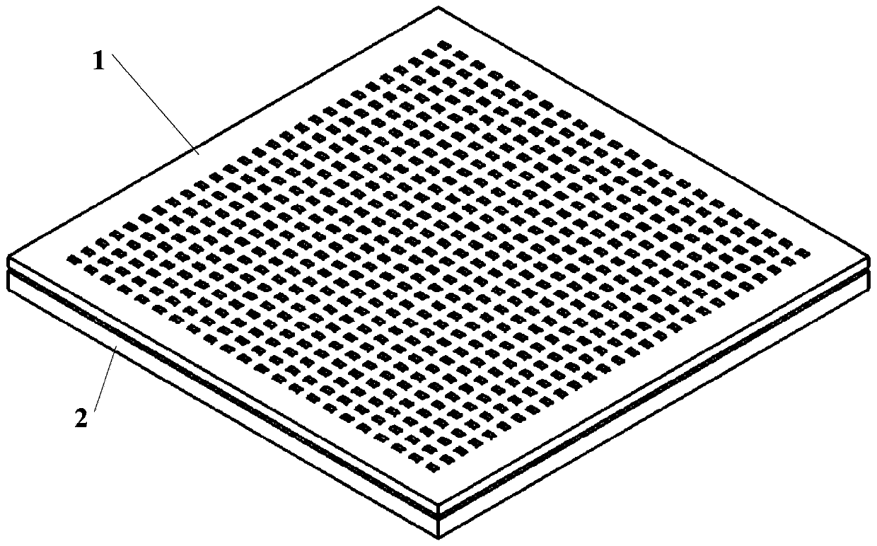
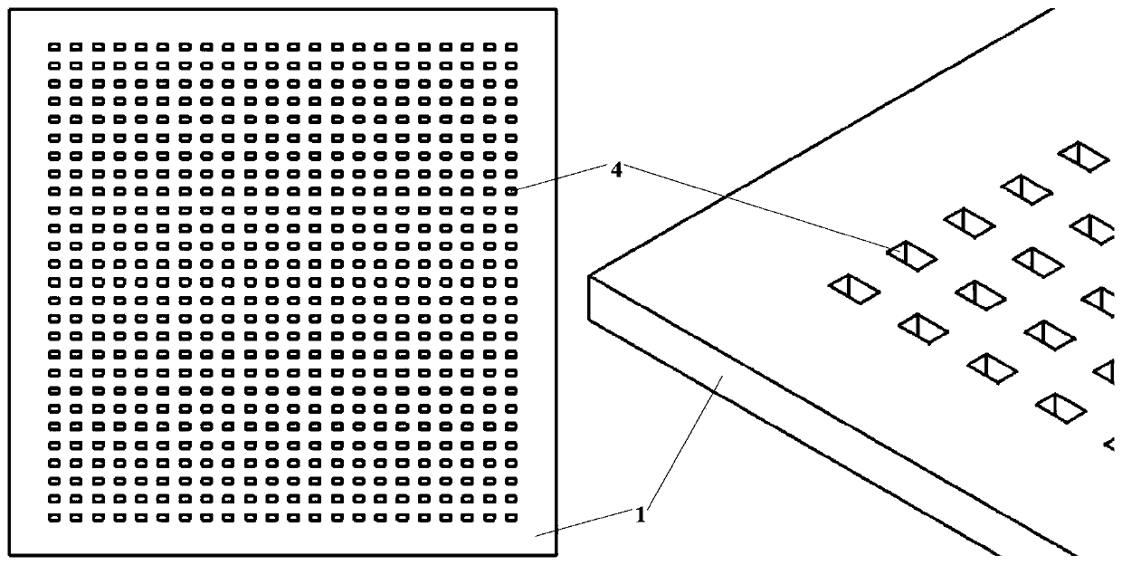
[0026] see Figure 1 to Figure 6 , the invention provides a size-adjustable bulk chip component mounting tray, comprising a loading array slot (1), a bottom hol...


PUM


Abstract

The invention provides a size-adjustable bulk chip component mounting tray, which includes a loading array slot, a bottom holding array and position adjustment screws; the loading array slot is provided with loading slots distributed in a rectangular array; the The bottom support array is arranged below the loading array tank, and the bottom support array is provided with guide protrusions distributed in a rectangular array, and the guide protrusions correspond to the upper and lower sides of the loading tank; the position adjustment The screw is used to adjust the distance between the loading array groove and the bottom holding array, so that the loading array groove can freely move up and down relative to the bottom holding array along the guide protrusion. During use, the relative position of the loading array slot and the bottom holding array can be adjusted by the position adjustment screw, thereby changing the depth of the loading slot to meet the placement requirements of the placement machine for bulk chip components of different thicknesses.

Description

technical field [0001] The invention relates to the technical field of electronic assembly, in particular to a size-adjustable bulk chip component mounting tray. Background technique [0002] With the extensive application of surface mount electronic components in the design process of printed circuit boards, the corresponding surface mount technology (SMT) has also made great progress. It not only realizes large-scale industrial production in the field of civilian products, but also gradually Aerospace, aviation, weapons and electronic systems and other military research have also been widely popularized and developed. [0003] Components of electronic products usually need to be screened before installation. During this process, the tapes that could have been used for mounting will be destroyed, resulting in the screening of bulk materials that cannot meet the mounting requirements of the placement machine. It has greatly affected the development of automatic placement eq...

Claims


Application Information

Patent Timeline
Patent Type & Authority Patents(China)
IPC IPC(8): H05K3/34
CPCH05K3/341
Inventor 张艳鹏王威石宝松
Owner CHANGCHUN INST OF OPTICS FINE MECHANICS & PHYSICS CHINESE ACAD OF SCI
Learn More