Display panel, display deVice and manufacturing method for display deVice

A display panel, display device technology, applied in the direction of static indicators, nonlinear optics, optics, etc.

Inactive Publication Date: 2018-10-19
GUANGDONG OPPO MOBILE TELECOMM CORP LTD
View PDF4 Cites 10 Cited by
  • Summary
  • Abstract
  • Description
  • Claims
  • Application Information

AI Technical Summary

Problems solved by technology

Therefore, under the existing chip on film (COF) technology, the lower border of the screen can only be 1.8mm, which is nearly double the size of the upper border (the upper border is generally about 0.8mm)

Method used


Image

  • Display panel, display deVice and manufacturing method for display deVice
  • Display panel, display deVice and manufacturing method for display deVice
  • Display panel, display deVice and manufacturing method for display deVice

Examples


Embodiment 1

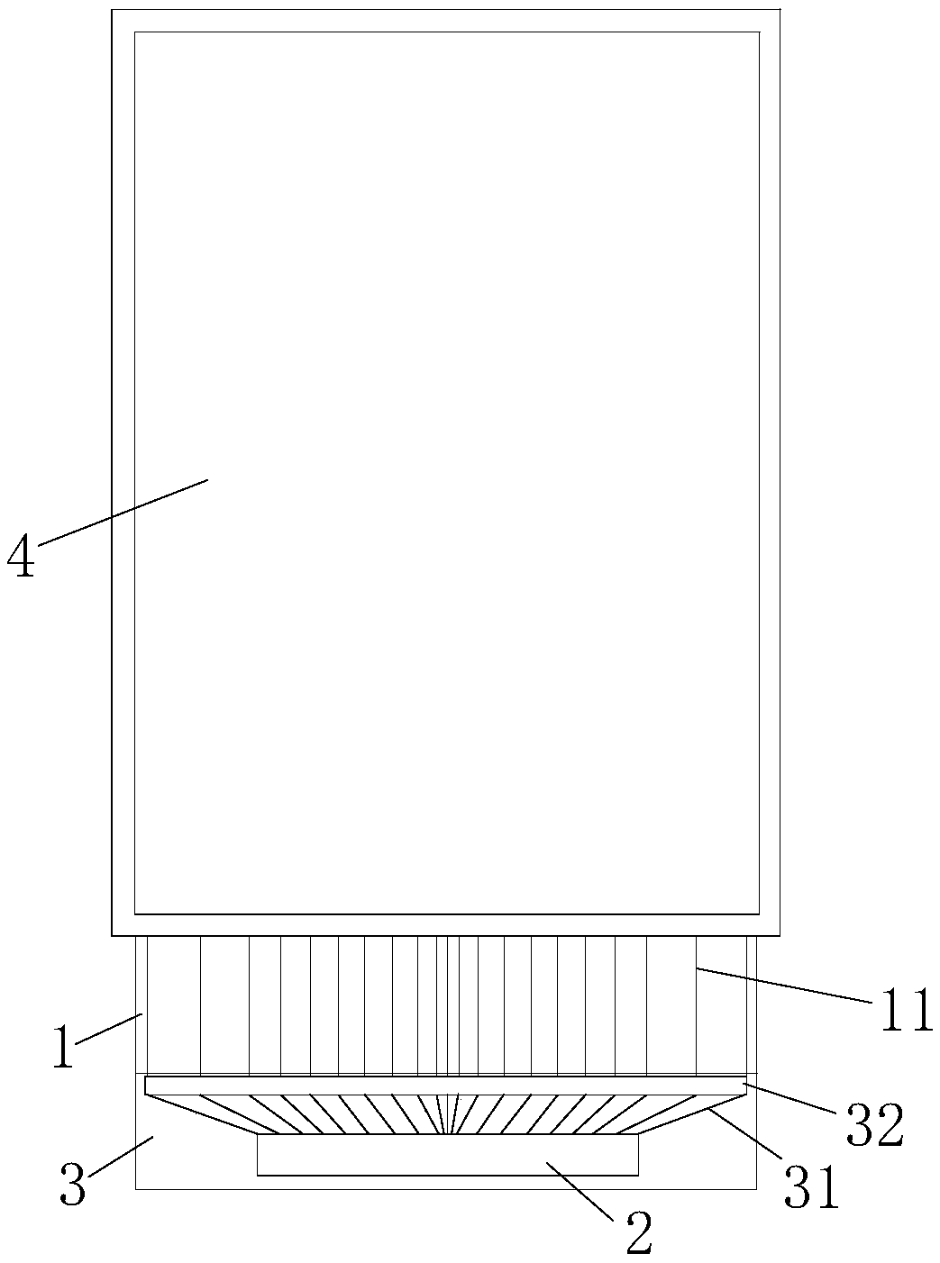
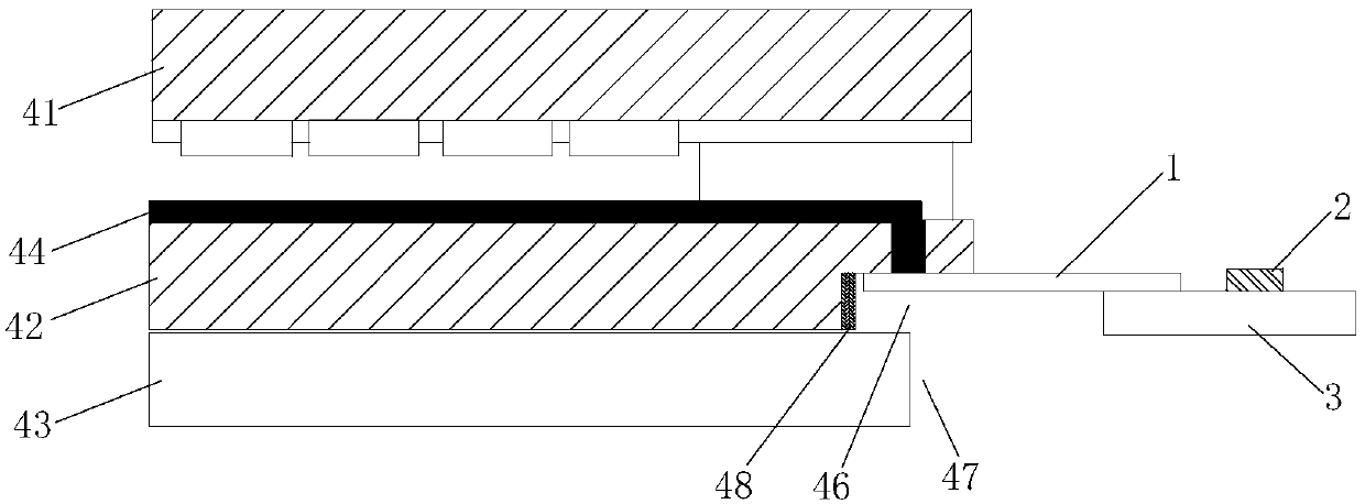
[0038] See Figure 1 to Figure 3 , a display device provided in this embodiment, including a circuit board 1 , an integrated circuit 2 , a loading substrate 3 and a display panel 4 .

[0039] Both ends of the circuit board 1 are bent in the same direction, the circuit board 1 is provided with a circuit 11 , and the loading substrate 3 is provided with a circuit 31 , a decomplexer circuit 32 and the integrated circuit 2 . The circuit 31 on the loading substrate 3 is electrically connected to the demultiplexer circuit 32 and the integrated circuit 2; the loading substrate 3 is located under the backlight layer. One end of the circuit 11 on the circuit board 1 is electrically connected to the signal line 44 on the display panel 4 , and the other end is electrically connected to the circuit 31 on the loading substrate 3 .

[0040] Optionally, the circuit board 1 is formed by folding a flexible circuit board, or, please refer to Figure 4 , the circuit board 1 can also be a rigid...

Embodiment 2

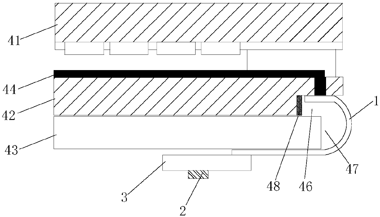
[0063] See Image 6 , is another display device provided by this embodiment, which includes a flexible circuit board 1', an integrated circuit 2 and a display panel 4.

[0064] The difference between this embodiment and the first embodiment is that this embodiment combines the loading substrate 3 and the circuit board 1 in the first embodiment into one flexible circuit board 1'.

[0065] Both ends of the flexible circuit board 1' in this embodiment are respectively provided with a binding area 13' and a loading area 14'. Both the binding area 13' and the loading area 14' are bent in the same direction, the wiring 11 is laid on the binding area 13', and the wiring 31, the demultiplexer circuit 32 and the integrated circuit 2 are laid on the loading area 13' . The loading area 14' is located below the backlight layer 43; the wiring 11 on the binding area 13' is electrically connected to the signal line 44 on the display panel 4, and the wiring 31 on the loading area 14' is con...


PUM


Abstract

The inVention is applicable to the technical field of displaying, and proVides a display panel, a display deVice and a manufacturing method for the display deVice. According to the display deVice, a fan-shaped stay wire originally arranged on the display panel and a recombiner circuit are arranged on a single loading substrate, an integrated circuit is also installed on the loading substrate, theloading substrate and the display panel are bound through a bending circuit board, therefore the loading substrate can be arranged below the display panel, and no influences on displaying can be caused; in addition, space at the side of the display panel cannot be occupied, therefore a lower frame of the display deVice can be made narrower, and the width of the lower frame is more close to or equal to the widths of other frames, and a full screen of which the four sides are same in width can be achieVed.

Description

technical field [0001] The invention belongs to the field of display technology, and in particular relates to a display panel, a display device and a manufacturing method of the display device. Background technique [0002] At present, display screens are more and more widely used in display products. Display products with narrow borders can make the products appear more fashionable and make people look more comfortable during use, attracting a large number of consumers. [0003] The lower frame of the liquid crystal display mainly includes a demultiplexer (Demux) circuit and fan-shaped pull wires. Therefore, under the existing chip on film (COF) technology, the lower border of the screen can only be 1.8mm, which is nearly double the size of the upper border (the upper border is generally about 0.8mm) . [0004] Therefore, how to make the width of the lower border of the display screen smaller is an urgent problem to be solved under the trend of narrow borders. Contents ...

Claims


Application Information

Patent Timeline
Patent Type & Authority Applications(China)
IPC IPC(8): G02F1/133G02F1/1333G02F1/1345
CPCG02F1/13306G02F1/133308G02F1/13452
Inventor 程才权游利军欧阳伟萍
Owner GUANGDONG OPPO MOBILE TELECOMM CORP LTD
Why Eureka
Try Eureka