
Optical modulator

A technology of light modulator and modulation part, applied in the directions of light guide, optics, instruments, etc., can solve the problem of low degree of freedom of wiring, and achieve the effect of simplifying the wiring structure

Active Publication Date: 2018-11-09
SUMITOMO OSAKA CEMENT CO LTD
View PDF9 Cites 2 Cited by
  • Summary
  • Abstract
  • Description
  • Claims
  • Application Information

AI Technical Summary

Problems solved by technology

However, in order to achieve both high performance, high density, and miniaturization of the optical modulator, the degree of freedom of wiring is limited due to the restriction of the size of the substrate, so it is necessary to study the wiring on the substrate.

Method used


Image

  • Optical modulator
  • Optical modulator
  • Optical modulator

Examples


Embodiment 1

[0042] figure 2 It is a plan view showing the optical modulator according to the first embodiment of the present invention.

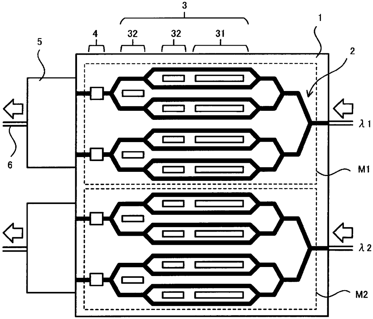
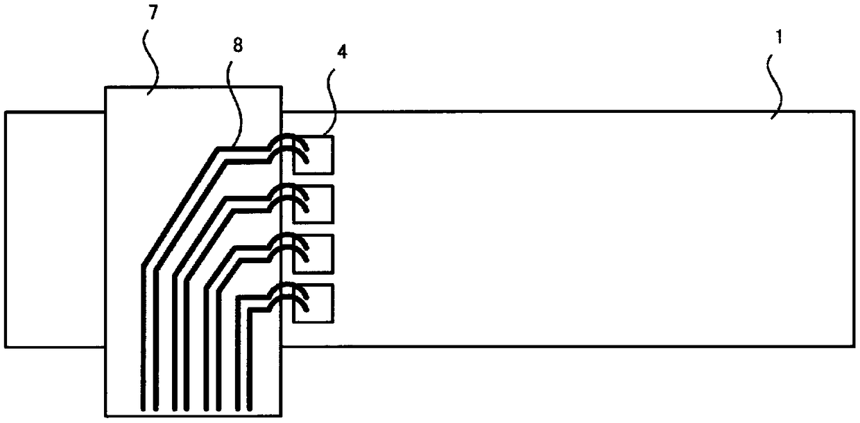
[0043] The optical modulator of this example includes a light receiving element 4 on the upper portion of the substrate 1 for each of the independent optical waveguide modulation sections. exist figure 2Among them, four light receiving elements 4 are provided on the substrate 1 . The wiring board 7 is separately arranged so as to be superimposed on the substrate 1 . The four light receiving elements 4 on the substrate 1 are arranged along one side of the wiring substrate 7 . On the upper surface of the wiring board 7 , a plurality of wirings 8 are arranged so as to extend to the vicinity of the side along which the light receiving elements 4 are arranged. The side end of each harness 8 is electrically connected to the light receiving element 4 corresponding to its arrangement position via a wire or the like. Each harness 8 extends toward the othe...

Embodiment 2

[0051] Figure 5 It is a plan view showing an optical modulator according to a second embodiment of the present invention.

[0052] In the light modulator of this example, the four light receiving elements 4 on the substrate 1 are arranged along opposite sides of the wiring substrate 7 . For example, the two light receiving elements 4 on the first optical waveguide modulator side are arranged along one of the two sides, and the two light receiving elements 4 on the second optical waveguide modulator side are arranged along the other side. On the upper surface of the wiring board 7 , a plurality of wirings 8 are arranged so as to extend to the vicinity of both sides along the arrangement of the light receiving elements 4 .

[0053] Also in such a configuration, the same effect as that of the light modulator of the above-mentioned embodiment can be obtained. In addition, since the light-receiving element of the first optical waveguide modulator and the light-receiving element ...

Embodiment 3

[0055] Figure 6 It is a plan view showing an optical modulator according to a third embodiment of the present invention.

[0056] The independent optical waveguide modulator of the optical modulator of this example is composed of a plurality of waveguide substrates 1 . That is, the first optical waveguide modulation section is constituted by the substrate 1a, and the second optical waveguide modulation section is constituted by the substrate 1b. In addition, two light receiving elements 4 are provided on the substrate 1a, and two light receiving elements 4 are provided on the substrate 1b. The substrates 1a, 1b are arranged side by side with each other on the same plane, and the wiring substrate 7 is arranged separately so as to overlap the substrates 1a, 1b. exist Figure 6 In the above, the four light receiving elements 4 on the substrates 1a and 1b are arranged along one side of the wiring board 7, but they may be arranged along opposite sides as in the second embodimen...


PUM


Abstract

To provide an optical modulator having a simplified wiring structure for a substrate on which an optical waveguide is formed. An optical modulator provided with: a substrate 1 having an electro-opticeffect; an optical waveguide 2 formed on the substrate 1; a plurality of control electrodes 3 for controlling optical waves propagating through the optical waveguide 2; and a plurality of light receiving elements 4 for detecting optical waves propagating through the optical waveguide 2; wherein the optical modulator has two or more independent optical waveguide modulating units; the light receiving element 4 is provided on an upper part of the substrate 1 with respect to each independent optical waveguide modulating unit; a wiring substrate 7 is present above the optical modulator; a pluralityof electric wires 8 are present on the wiring substrate 7; and the plurality of electric wires 8 are disposed extending to near one side of the wiring substrate 7, are electrically connected to the light receiving elements 4, and output, to the outside, signals detected by the light receiving elements 4.

Description

technical field [0001] The present invention relates to an optical modulator, and more particularly to a wiring structure of a two-wavelength integrated modulator and other highly integrated modulators. Background technique [0002] As the speed and capacity of optical communication systems increase, the performance and density of optical modulators used in optical communication systems are increasing. In addition, along with the demand for miniaturization of optical modulators, miniaturization of substrates constituting optical modulators is also progressing. However, in order to achieve both high performance, high density, and miniaturization of the optical modulator, the degree of freedom of wiring is limited due to the restriction of the size of the substrate, and therefore it is necessary to study the wiring on the substrate. [0003] Regarding the wiring of such an optical modulator, the following inventions have been proposed. [0004] For example, Patent Documents ...

Claims


Application Information

Patent Timeline
Patent Type & Authority Applications(China)
IPC IPC(8): G02F1/03G02F1/035
CPCG02B6/4286G02B6/428G02F1/035G02F1/011G02F1/225G02F1/025G02F1/03G02F1/212
Inventor 宫崎德一加藤圭
Owner SUMITOMO OSAKA CEMENT CO LTD
Features
  • Generate Ideas
  • Intellectual Property
  • Life Sciences
  • Materials
  • Tech Scout
  • Unparalleled Data Quality
  • Higher Quality Content
  • 60% Fewer Hallucinations
Learn More