A Film sensor ITO pattern and a manufacturing method thereof

A manufacturing method and graphic technology, applied in the field of ITO thin film sensor, can solve the problems of ITO damage, poor function, poor appearance, etc., and achieve the effect of avoiding appearance and reducing electrostatic damage

Inactive Publication Date: 2018-12-11
SHENZHEN SUCCESS ELECTRONICS LTD +3
View PDF6 Cites 0 Cited by
  • Summary
  • Abstract
  • Description
  • Claims
  • Application Information

AI Technical Summary

Problems solved by technology

[0003] In order to solve the above problems, the object of the present invention is to provide a Film sensor ITO pattern and a manufacturing method thereof, which can better protect and transfer the bad electrostatic damage produced in the Film sensor production process, and avoid ITO damage caused by static electricity, Breakage, dirt phenomenon, thereby reducing the risk of poor function, poor appearance

Method used


Image

  • A Film sensor ITO pattern and a manufacturing method thereof

Examples


Embodiment 1

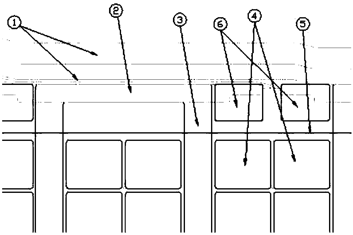
[0028] Example 1, such as figure 1 As shown, a Film sensor ITO pattern according to an embodiment of the present invention includes: an ITO channel pattern 3 etched on an ITO conductive film, an ITO Dummy block pattern 4, a conductive silver paste pattern 1 and an ITO Dummy block pattern 6 added. Wherein, the ITO conductive thin film is deposited on the Film substrate, including a substrate layer and an ITO layer disposed on the substrate layer. The window area 5 of the ITO layer is provided with an ITO channel area and an ITO pattern area. The ITO channel pattern 3 is etched in the ITO channel area. The ITO Dummy block pattern 4 is etched in the ITO pattern area, and the ITO Dummy block pattern 4 is located between the ITO channel patterns 3 . The conductive silver paste pattern 1 is located in the frame area surrounding the window area 5 and is connected to the ITO channel pattern 3 . The ITO Dummy block pattern 6 is added and etched on the ITO layer, and is located at th...

Embodiment 2

[0034] Embodiment 2, a kind of making method of Film sensor ITO figure, comprises the following steps:

[0035] Step 1, forming an ITO layer on the Film substrate;

[0036] Step 2, etching the ITO channel pattern 3 and the ITO Dummy block pattern 4 in the window area 5 on the ITO layer, and the ITODummy block pattern 4 is located between the ITO channel patterns 3;

[0037] Step 3, printing conductive silver paste on the ITO layer around the frame area of ​​the window area 5, and etching the conductive silver paste pattern 1, and the conductive silver paste pattern 1 is connected to the ITO channel pattern 3;

[0038] Step 4: Etch an additional ITO Dummy block pattern 6 at the overlap between the conductive silver paste pattern 1 on the ITO layer and the ITO channel region.

[0039] Among them, the ITO channel pattern 3, the ITO Dummy block pattern 4 and the added ITO Dummy block pattern 6 are all etched into periodically arranged patterns. ITO Channel Graphics 3, ITO Dummy ...


PUM


Abstract

The invention discloses a Film sensor ITO pattern, comprising: an ITO channel pattern etched on an ITO layer of an ITO conductive thin film in an ITO channel region in a window region; an ITO Dummy block pattern etched on the ITO layer of the ITO conductive film in the ITO pattern region in the window region between the ITO channel patterns; and an electrically conductive silver paste pattern located in a frame region surrounding the window region and in communication with the ITO channel pattern. The ITO Dummy block pattern, which is additionally adopted, is etched on the ITO layer and located at the junction of the conductive silver paste pattern and the ITO channel region. The ITO conductive film is deposited on a Film substrate and includes a substrate layer and an ITO layer disposed on the substrate layer. The invention also provides a manufacturing method of a Film sensor ITO pattern. The invention has the beneficial effects of exhibiting better protection and transfer performance of static electricity damage generated in the production process of the Film sensor, avoiding ITO damage, fracture and dirt phenomenon caused by static electricity, and reducing the risk of poor function and poor appearance.

Description

technical field [0001] The invention relates to the technical field of ITO film sensor, in particular to a Film sensor ITO pattern and a manufacturing method thereof. Background technique [0002] At present, most smartphones use ITO film materials to make touch sensors, which are used to make external touch panels to realize touch functions. When manufacturers mostly use the R2R process, electrostatic damage to ITO often occurs, resulting in ITO damage, dirt in the window area, resulting in poor appearance, and serious ITO disconnection, resulting in malfunction. Contents of the invention [0003] In order to solve the above problems, the object of the present invention is to provide a Film sensor ITO pattern and a manufacturing method thereof, which can better protect and transfer the bad electrostatic damage produced in the Film sensor production process, and avoid ITO damage caused by static electricity, Breakage, dirt phenomenon, thereby reducing the risk of poor fun...

Claims


Application Information

Patent Timeline
Patent Type & Authority Applications(China)
IPC IPC(8): G06F3/041
CPCG06F3/041G06F2203/04103
Inventor 沈涛黄效牛左洪冯佑胜
Owner SHENZHEN SUCCESS ELECTRONICS LTD
Why Eureka
Try Eureka