Thin film transistor array substrate and liquid crystal dispaly panel

A thin film transistor and array substrate technology, applied in the field of element array substrates and display panels, can solve the problems of electrostatic damage, large area, easy accumulation of large static electricity, etc., and achieve the effect of reducing the phenomenon of electrostatic damage

Active Publication Date: 2009-04-08
WUHAN CHINA STAR OPTOELECTRONICS TECH CO LTD
View PDF7 Cites 0 Cited by
  • Summary
  • Abstract
  • Description
  • Claims
  • Application Information

AI Technical Summary

Problems solved by technology

[0009] However, only by using the above-mentioned design of the inner electrostatic protection ring 192 and the outer electrostatic protection ring 194, electrostatic damage may still occur, especially at the positions of the scanning pad 160 and the data pad 170 because of their large area. It is particularly easy to accumulate a large amount of static electricity
Therefore, when the static electricity cannot be vented, the lines on the thin film transistor array substrate 100 or the thin film transistors 152 will still be damaged by static electricity.

Method used


Image

  • Thin film transistor array substrate and liquid crystal dispaly panel
  • Thin film transistor array substrate and liquid crystal dispaly panel
  • Thin film transistor array substrate and liquid crystal dispaly panel

Examples


Embodiment Construction

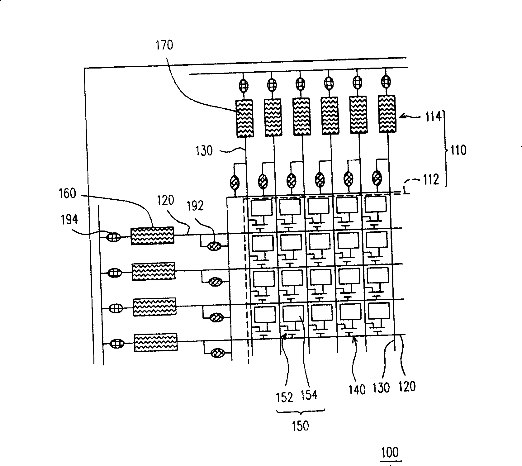
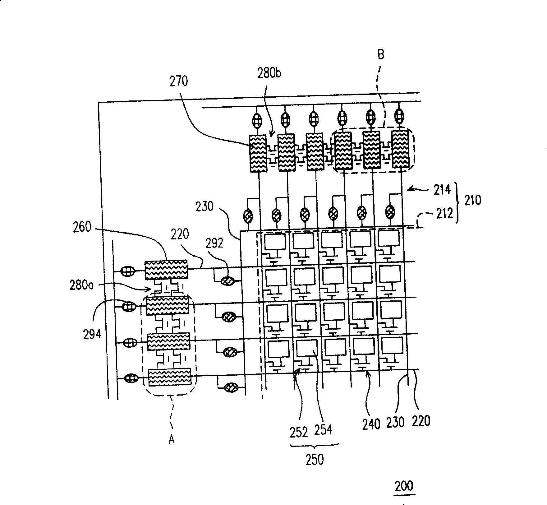
[0062] figure 2 It is a schematic diagram of a thin film transistor array substrate according to a preferred embodiment of the present invention. Please refer to figure 2 , the TFT array substrate 200 includes a substrate 210, a plurality of scan lines 220 and data lines 230, a plurality of pixel units 250, a plurality of scan pads 260 and data pads 270, a plurality of first switching elements 280a and a plurality of second Two switching elements 280b.

[0063] The substrate 210 has a display area 212 and a peripheral circuit area 214 . The scan lines 220 and the data lines 230 are disposed on the substrate 210 , wherein the scan lines 220 and the data lines 230 divide the display area 212 into a plurality of pixel areas 240 . Each pixel unit 250 is disposed in one of the pixel regions 240 and driven by the scan line 220 and the data line 230 . The scan pad 260 is disposed in the peripheral circuit area 214 , and the scan pad 260 is electrically connected to the scan lin...


PUM


Abstract

A substrate of film transistor array consists of substrate having display and peripheral circuit region on base plate, arranging scan line and data line on substrate, driving display region to be multiple pixel region with pixel unit being driven by said scan and data lines, setting scan welding pad and data welding pad in peripheral circuit region and connecting them to scan and data lines, setting the first and the second switch elements in said circuit region as the first switch element being set between two adjacent scan welding pads and the second switch element being set between two adjacent data welding pads.

Description

technical field [0001] The present invention relates to a device array substrate (device array substrate) and a display panel (display panel), and in particular to a thin film transistor array substrate (Thin Film Transistor array substrate, TFT array substrate) with anti-static capability (anti-static capability) ) and liquid crystal display panel (Liquid Crystal Display panel, LCD panel). Background technique [0002] In recent years, due to the maturity of optoelectronic technology and semiconductor manufacturing technology, the flat panel display (Flat Panel Display) has been vigorously developed, among which thin film transistor liquid crystal display (Thin FilmTransistor Liquid Crystal Display, TFT-LCD) is based on its low voltage operation, operation speed Due to the advantages of high speed, light weight and small size, it has gradually become the mainstream of display products. [0003] TFT liquid crystal display mainly includes a liquid crystal display panel and a...

Claims


Application Information

Patent Timeline
Patent Type & Authority Patents(China)
IPC IPC(8): G02F1/1368H01L29/786
Inventor 刘文雄沈慧中洪孟锋
Owner WUHAN CHINA STAR OPTOELECTRONICS TECH CO LTD
Why Eureka
Try Eureka