
Pixel driving circuit and liquid crystal display device

A pixel driving circuit, pixel technology, applied in static indicators, nonlinear optics, instruments, etc., can solve the problems of abnormal screen display, different voltage values, deviation from voltage values, etc., to improve display quality, good display quality, and voltage Value consistent effect

Inactive Publication Date: 2018-12-21
TCL CHINA STAR OPTOELECTRONICS TECH CO LTD
View PDF5 Cites 8 Cited by
  • Summary
  • Abstract
  • Description
  • Claims
  • Application Information

AI Technical Summary

Problems solved by technology

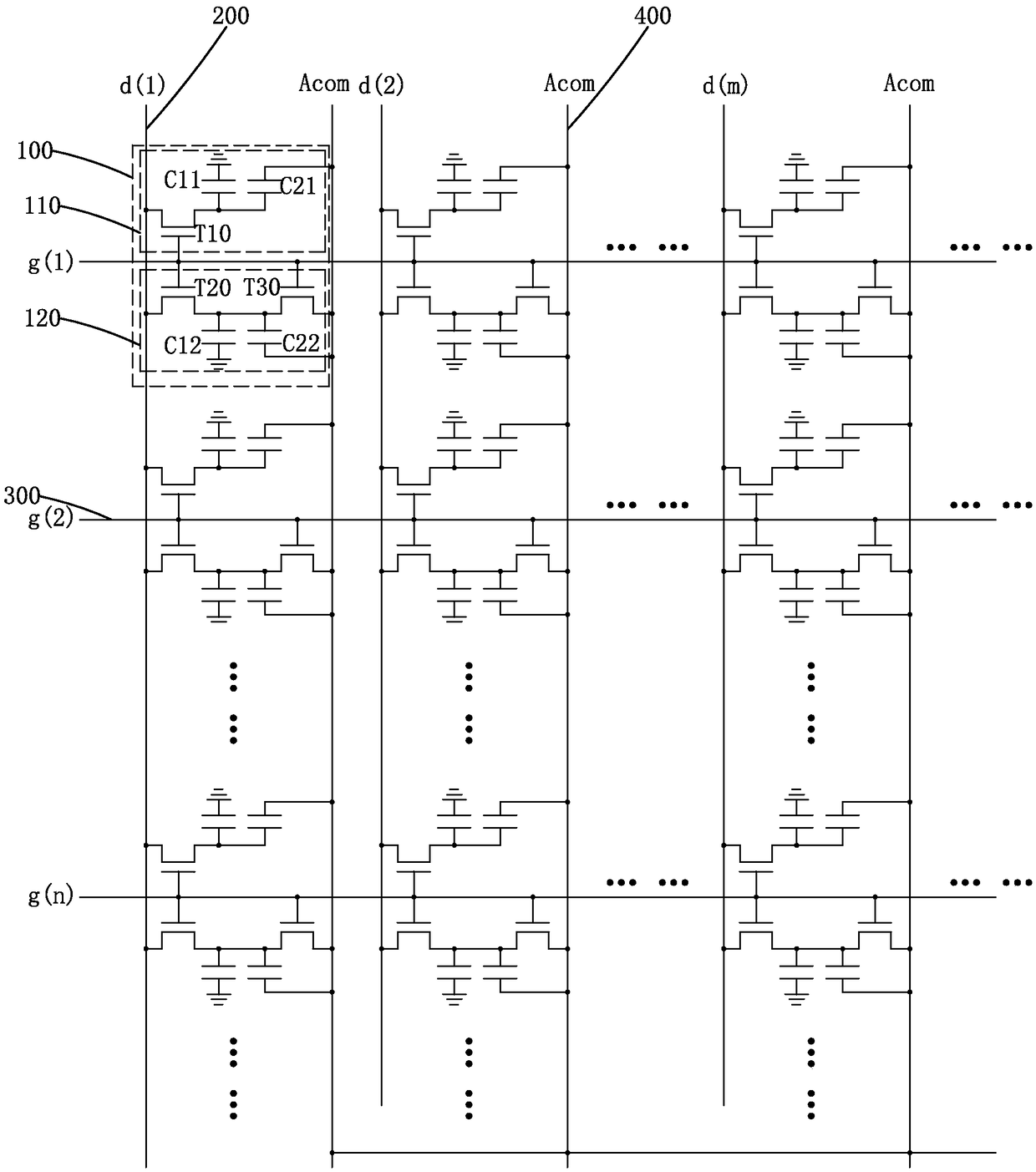
However, figure 1 In the pixel driving circuit shown, since the voltage at one end of the second liquid crystal capacitor C12 is released to the common voltage line 400 of the array substrate, the common voltage Acom of the array substrate on the common voltage line 400 of the array substrate will change and deviate from the initially set voltage. value, resulting in different voltage values ​​in different areas on the common voltage line 400 of the array substrate, resulting in abnormal screen display

Method used


Image

  • Pixel driving circuit and liquid crystal display device
  • Pixel driving circuit and liquid crystal display device
  • Pixel driving circuit and liquid crystal display device

Examples


Embodiment Construction

[0027] In order to further illustrate the technical means adopted by the present invention and its effects, the following describes in detail in conjunction with preferred embodiments of the present invention and accompanying drawings.

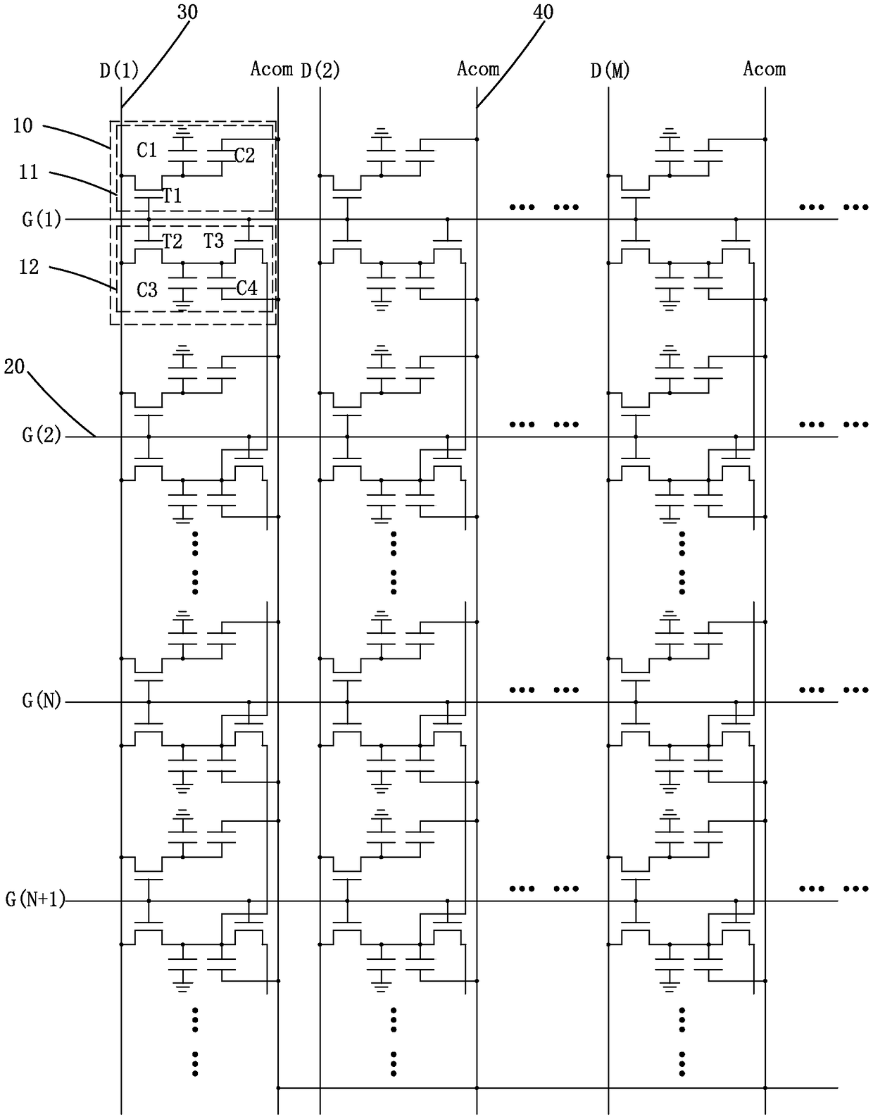
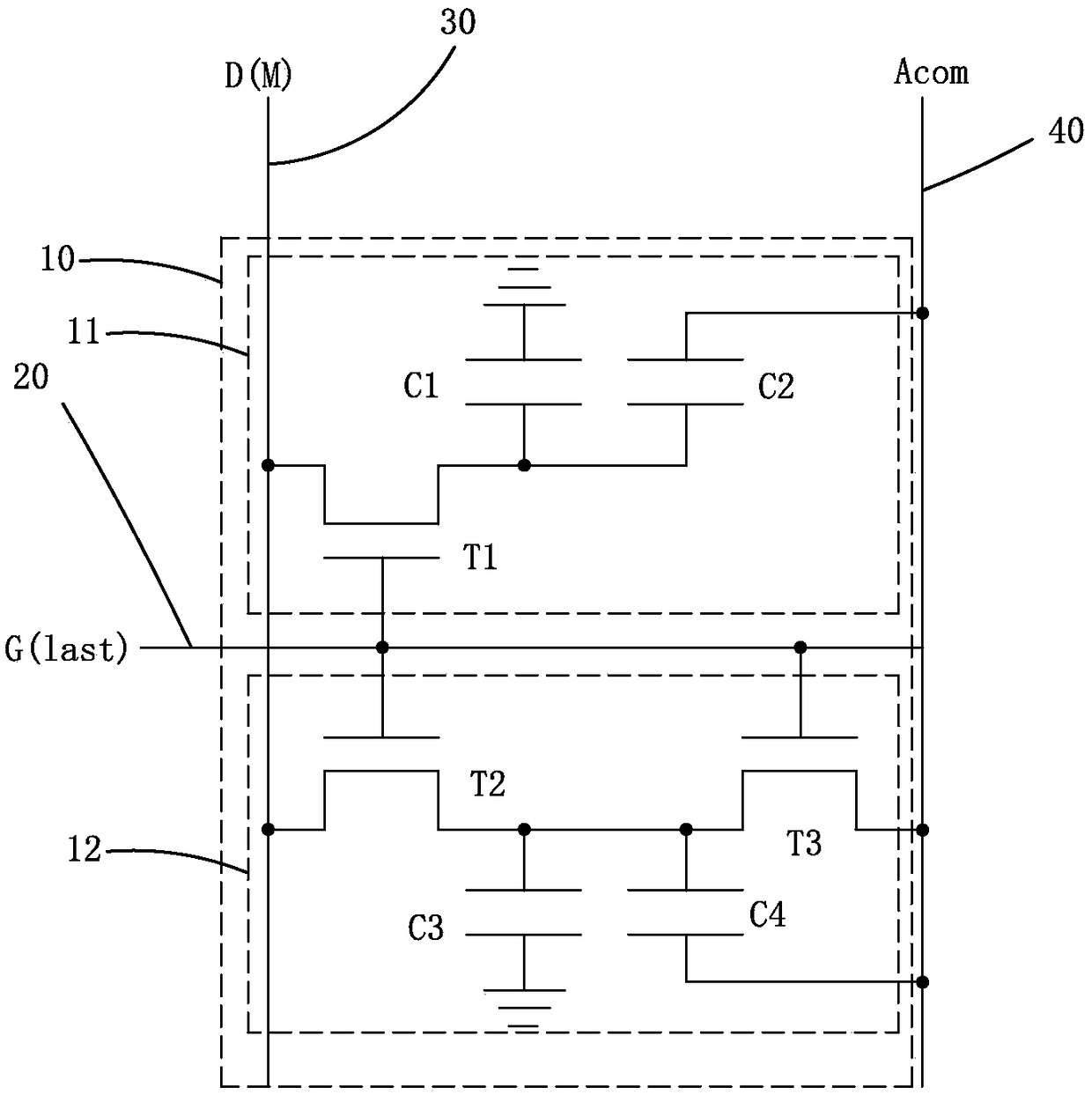
[0028] see figure 2 , and combined with image 3 or Figure 4 , the present invention provides a pixel driving circuit, including a plurality of sub-pixels 10 arranged in an array, and a plurality of scanning lines 20 (G(1), G(2)...G(N) respectively corresponding to multiple rows of sub-pixels 10 , G(N+1)...), a plurality of data lines 30 (D(1), D(2)...D(M)...) respectively corresponding to multiple columns of sub-pixels 10, and a common voltage line 40 of the array substrate .

[0029] The sub-pixel 10 includes a first TFT T1, a first liquid crystal capacitor C1, a first storage capacitor C2, a second TFT T2, a third TFT T3, a second liquid crystal capacitor C3 and a second storage capacitor C4. The area where the first thin film transis...


PUM


Abstract

The invention provides a pixel driving circuit and a liquid crystal display device. The pixel driving circuit electrically connects drains of third thin film transistors of each sub-pixel of the Nth row of sub-pixels with the first end of a second liquid crystal capacitor of a sub-pixel of the (N+1)th row of sub-pixels correspondingly, so that, when scanning the Nth row of sub-pixels during driving, the third thin film transistors of the Nth row of sub-pixels turn on to release the voltage of the first end of the second liquid crystal capacitor of the Nth row of sub-pixels to the first end ofthe second liquid crystal capacitor of the (N+1)th row of sub-pixels, without affecting the voltage on the common voltage line of an array substrate, thereby effectively ensuring consistency of voltage values of each region on the common voltage line of the array substrate, and is applicable to a liquid crystal display device for improving display quality of the liquid crystal display device.

Description

technical field [0001] The invention relates to the field of display technology, in particular to a pixel driving circuit and a liquid crystal display device. Background technique [0002] Liquid Crystal Display (LCD) has many advantages such as thin body, power saving, and no radiation, and has been widely used, such as: LCD TV, mobile phone, personal digital assistant (PDA), digital camera, computer screen or Laptop screens, etc., dominate the field of flat panel displays. [0003] Most of the liquid crystal displays currently on the market are backlight liquid crystal displays, which include a liquid crystal display panel and a backlight module. The working principle of the liquid crystal display panel is to pour liquid crystal molecules between the thin film transistor substrate (Thin FilmTransistor Array Substrate, TFT Array Substrate) and the color filter substrate (Color Filter, CF), and apply a driving voltage on the two substrates to Control the rotation direction...

Claims


Application Information

Patent Timeline
Patent Type & Authority Applications(China)
IPC IPC(8): G02F1/1362G02F1/1368G02F1/133G09G3/36
CPCG02F1/13306G02F1/136286G02F1/1368G09G3/3648G02F1/13624G09G2300/0426G09G2300/0447G09G2300/0852G09G2320/0242G02F1/133514
Inventor 刘司洋
Owner TCL CHINA STAR OPTOELECTRONICS TECH CO LTD
Learn More