A SRAM memory cell circuit with low bit line leakage current

A technology of memory cell circuit and leakage current, applied in the field of memory array and SRAM memory cell circuit, can solve the problems of easy failure of write operation, limited read and write ability, read interference, etc., and achieve high write margin, save area and power consumption , the effect of low static power consumption

Active Publication Date: 2021-08-03
UNIV OF ELECTRONICS SCI & TECH OF CHINA
View PDF6 Cites 0 Cited by
  • Summary
  • Abstract
  • Description
  • Claims
  • Application Information

AI Technical Summary

Problems solved by technology

[0003] At present, the mainstream unit of SRAM is 6T structure, such as figure 1 Shown is a schematic diagram of the traditional 6T SRAM storage unit circuit structure. In order to make the 6T SRAM storage unit have higher stability, the size of the tube can be optimized, but the read and write capabilities of the tube of the optimized 6TSRAM storage unit are limited, and due to There is a competition between the data to be written and the saved data value, and the write operation is prone to failure at low voltage. If the 6T unit is used in the bit interleaved structure, it will cause read interference and write half-selection problems

Method used


Image

  • A SRAM memory cell circuit with low bit line leakage current
  • A SRAM memory cell circuit with low bit line leakage current
  • A SRAM memory cell circuit with low bit line leakage current

Examples


Embodiment Construction

[0026] The present invention will be described in detail below in conjunction with the accompanying drawings and application examples.

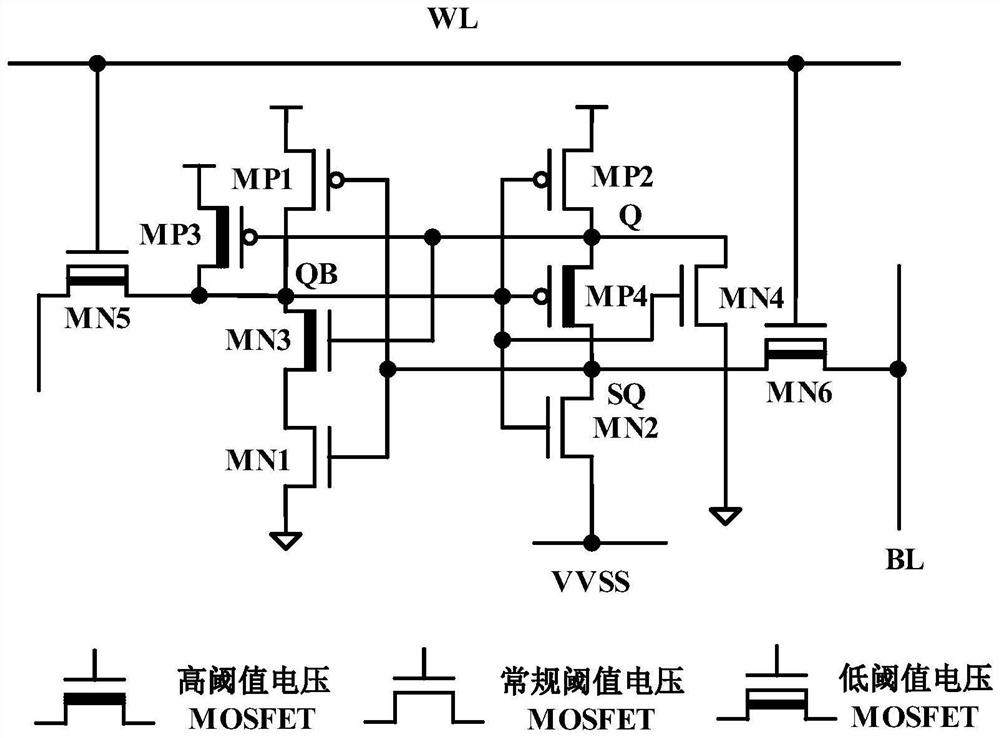
[0027] The SRAM storage unit circuit of the low bit line leakage current proposed by the present invention is a 10T structure, and its specific circuit structure is as follows figure 2 As shown, it includes the first NMOS transistor MN1, the second NMOS transistor MN2, the third NMOS transistor MN3, the fourth NMOS transistor MN4, the fifth NMOS transistor MN5, the sixth NMOS transistor MN6, the first PMOS transistor MP1, the second PMOS transistor MP2, the third PMOS transistor MP3 and the fourth PMOS transistor MP4, wherein in order to improve the read and write performance of the SRAM storage unit circuit, the third NMOS transistor MN3, the third PMOS transistor MP3 and the fourth PMOS transistor MP4 can be set as high threshold MOS The fifth NMOS transistor MN5 and the sixth NMOS transistor MN6 are set as low-threshold MOS transistors; t...


PUM


Abstract

The invention relates to an SRAM storage unit circuit with low bit line leakage current, which belongs to the technical field of integrated circuits. The drain of the fifth NMOS transistor is connected to the shared bit line, its gate is connected to the gate of the sixth NMOS transistor and connected to the word line, its source is connected to the drains of the third NMOS transistor, the first PMOS transistor and the third PMOS transistor, and The gate of the second NMOS transistor, the fourth NMOS transistor, the second PMOS transistor and the fourth PMOS transistor; the gate of the first NMOS transistor is connected to the gate of the first PMOS transistor, the source of the sixth NMOS transistor and the second NMOS transistor tube and the drain of the fourth PMOS tube, its drain is connected to the source of the third NMOS tube, its source is connected to the source of the fourth NMOS tube and grounded; the source of the second PMOS tube is connected to the first PMOS tube and the first PMOS tube The sources of the three PMOS transistors are connected to the power supply voltage, and their drains are connected to the source of the fourth PMOS transistor, the drain of the fourth NMOS transistor, and the gates of the third NMOS transistor and the third PMOS transistor; the source of the second NMOS transistor The pole is connected to the control signal line, and the drain of the sixth NMOS transistor is connected to the bit line. The invention has the characteristics of high read noise tolerance, high write margin, high stability and low static power consumption.

Description

technical field [0001] The invention relates to the technical field of integrated circuits, in particular to an SRAM storage unit circuit with low bit line leakage current, and a storage array composed of the SRAM storage unit circuit. Background technique [0002] The low-voltage design is widely used because of its low power consumption, especially for high-density integrated circuits such as SRAM memory cells. However, as the power supply voltage decreases, SRAM memory cells are more significantly affected by process fluctuations, resulting in reduced read and write stability of SRAM memory cells and even errors, which place higher requirements on the design of SRAM memory cells. At the same time, with the continuous shrinking of the process size and the increase of the storage capacity, the soft error rate of the memory becomes higher and higher. The traditional error correction coding technology can only solve the single-bit soft error rate. As the process node enters ...

Claims


Application Information

Patent Timeline
Patent Type & Authority Patents(China)
IPC IPC(8): G11C16/04
CPCG11C16/0466
Inventor 贺雅娟张九柏吴晓清张子骥张波
Owner UNIV OF ELECTRONICS SCI & TECH OF CHINA
Why Eureka
Try Eureka