SRAM memory cell circuit with high reading noise margin

A storage unit circuit and noise tolerance technology, applied in information storage, static memory, digital memory information, etc., can solve problems such as unrealistic design goals and difficult writing operations, improve soft error rate problems, and solve half-selection problems problem, effect of high read noise margin

Active Publication Date: 2018-11-06
UNIV OF ELECTRONIC SCI & TECH OF CHINA
View PDF6 Cites 3 Cited by
  • Summary
  • Abstract
  • Description
  • Claims
  • Application Information

AI Technical Summary

Problems solved by technology

[0004] At present, the mainstream unit of SRAM is 6T structure, such as figure 1 Shown is a schematic diagram of the circuit structure of a traditional 6T SRAM storage unit. When 6T is used in a bit-interleaved structure, it will cause a half-selection problem. At a lower voltage, the write operation becomes difficult.
Certain design needs can be met by adjusting the device size, but it has become unrealistic to achieve the design goal simply by adjusting the device size, and the improvement of the read noise margin and the improvement of the write margin are contradictory

Method used


Image

  • SRAM memory cell circuit with high reading noise margin
  • SRAM memory cell circuit with high reading noise margin
  • SRAM memory cell circuit with high reading noise margin

Examples


Embodiment Construction

[0020] The present invention will be described in detail below in conjunction with the accompanying drawings and specific embodiments.

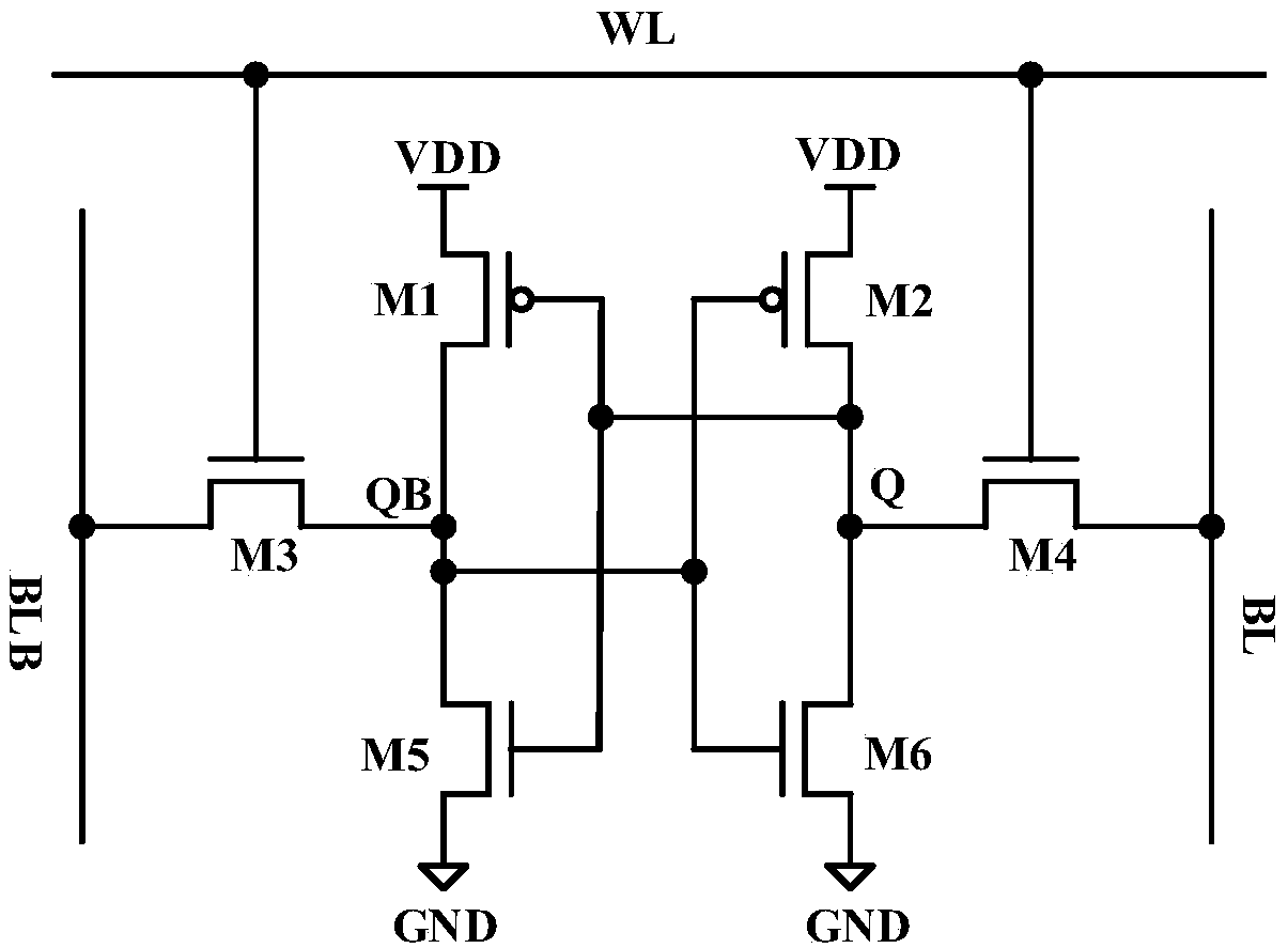
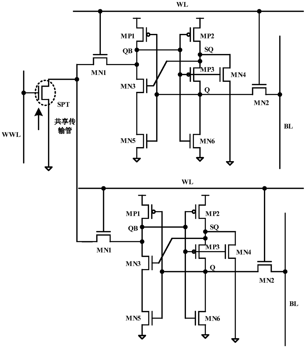
[0021] The SRAM storage unit circuit proposed by the present invention has a 9T structure, including a first NMOS transistor MN1, a second NMOS transistor MN2, a third NMOS transistor MN3, a fourth NMOS transistor MN4, a fifth NMOS transistor MN5, a sixth NMOS transistor MN6, The first PMOS transistor MP1, the second PMOS transistor MP2 and the third PMOS transistor MP3, the gate of the first NMOS transistor MN1 is connected to the gate of the second NMOS transistor MN2 and the word line WL, its drain serves as a shared transmission terminal, and its source The poles are connected to the gates of the second PMOS transistor MP2, the third PMOS transistor MP3, the fourth NMOS transistor MN4 and the sixth NMOS transistor MN6 and the drains of the first PMOS transistor MP1 and the third NMOS transistor MN3; the second NMOS transistor MN2 The drai...


PUM


Abstract

The invention discloses an SRAM memory cell circuit with high reading noise margin and belongs to the technical field of integrated circuits. A grid of a first NMOS transistor is connected with a gridof a second NMOS transistor and a word line, a drain of the first NMOS transistor is used as a shared transmission end, and a source of the first NMOS transistor is connected with grids of a second PMOS transistor, a third PMOS transistor, a fourth NMOS transistor and a sixth NMOS transistor and drains of a first PMOS transistor and a third NMOS transistor; a drain of the second NMOS transistor is connected with a bit line, and a source of the second NMOS transistor is connected with grids of the first PMOS transistor and a fifth NMOS transistor and drains of the third PMOS transistor and a sixth NMOS transistor; a source of the second PMOS transistor is connected with a source of the first PMOS transistor and power voltage, and a drain of the second PMOS transistor is connected with a grid of the third NMOS transistor, a source of the third PMOS transistor and a drain of the fourth NMOS transistor; a drain of the fifth NMOS transistor is connected with a source of the third NMOS transistor, and a source of the fifth NMOS transistor is connected with sources of the fourth NMOS transistor and the sixth NMOS transistor and grounded. The circuit has higher reading noise margin, can solve the half selection and can solve the problem about soft error rate of memories in bit interleaving array structures.

Description

technical field [0001] The invention relates to the technical field of integrated circuits, in particular to an SRAM storage unit circuit with high read noise tolerance, which can be applied to a bit interleaving structure to solve the half-selection problem. Background technique [0002] In recent years, application fields represented by wireless sensor networks and medical electronic equipment have higher and higher requirements for power consumption and performance of SoCs. Embedded static random access memory (SRAM) is one of the key components of SoCs. Reducing the power supply voltage is an effective means to ensure low power consumption of SRAM. However, the reduction of power supply voltage will bring some bad effects, such as reducing the stability of reading and writing. Therefore, one of the criteria for designing low-voltage SRAM is to improve the reading and writing of cells. performance. [0003] Another criterion for low-voltage SRAM cell design is to solve t...

Claims


Application Information

Patent Timeline
IPC IPC(8): G11C11/419
CPCG11C11/419
Inventor 贺雅娟吴晓清张九柏衣溪琳钱亦端裴浩然张波
Owner UNIV OF ELECTRONIC SCI & TECH OF CHINA
Why Eureka
Try Eureka