A Subthreshold SRAM Memory Cell Circuit Solving the Half-selection Problem

A storage unit circuit and sub-threshold technology, which is applied in information storage, static memory, digital memory information, etc., can solve the problem of affecting the potential of storage points, the limited improvement of 6T unit read and write capabilities, and the reduced stability of read half-select and write half-select And other issues

Inactive Publication Date: 2020-10-27
UNIV OF ELECTRONIC SCI & TECH OF CHINA
View PDF6 Cites 0 Cited by
  • Summary
  • Abstract
  • Description
  • Claims
  • Application Information

AI Technical Summary

Problems solved by technology

However, the use of the bit interleaving structure will cause half-selection problems, including the reduction of the stability of read half-selection and write half-selection, and even destroy the original storage state of the memory.
[0003] At present, the mainstream unit of SRAM is 6T structure, such as figure 1 Shown is a schematic diagram of the traditional 6T SRAM storage unit circuit structure. In order to make the 6T unit more stable, the size of the tube can be optimized, but the read and write capabilities of the optimized 6T unit are limited.
If the 6T unit is used in the bit-interleaved structure, the semi-selected unit will cause the transmission transistors N3 and N4 to open because the bit line WWL is at a high level, so the change of the bit line BL and BLB will affect the potential of the storage point, resulting in a half-selection problem.

Method used


Image

  • A Subthreshold SRAM Memory Cell Circuit Solving the Half-selection Problem
  • A Subthreshold SRAM Memory Cell Circuit Solving the Half-selection Problem
  • A Subthreshold SRAM Memory Cell Circuit Solving the Half-selection Problem

Examples


Embodiment Construction

[0020] The present invention will be described in detail below in conjunction with the accompanying drawings and specific embodiments.

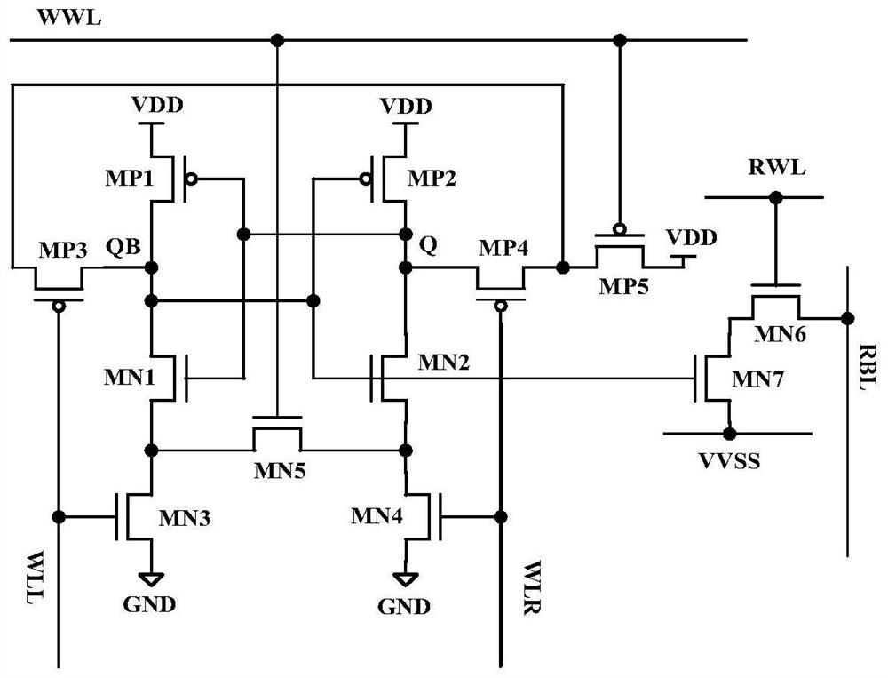
[0021] Such as figure 2 Shown is a schematic structural diagram of a sub-threshold SRAM memory cell circuit that solves the half-selection problem provided by the present invention, wherein the drain of the second PMOS transistor MP2 is the first storage point Q, and the drain of the first PMOS transistor MP1 is the second storage point QB; the first PMOS transistor MP1 and the first NMOS transistor MN1 constitute the first inverter, and the second PMSO transistor MP2 and the second NMOS transistor MN2 constitute the second inverter for storing opposite data, that is, storage points Q and To store the data of point QB, two inverters form a feedback structure, so that the data is stably latched. The first signal control line WLL, the second signal control line WLR and the third signal control line VVSS are used to control the circuit of the ...


PUM


Abstract

The invention relates to a sub-threshold SRAM storage unit circuit for solving the half-selection problem, which belongs to the technical field of integrated circuits. In the memory cell circuit provided by the present invention, the first PMOS transistor MP1 and the first NMOS transistor MN1 constitute the first inverter, and the second PMSO transistor MP2 and the second NMOS transistor MN2 constitute the second inverter for storing opposite data. , two inverters form a feedback structure, so that the data can be latched stably; the sixth NMOS transistor MN6 and the seventh PMOS transistor MN7 are used to control the read operation, and the fifth NMOS transistor MN5 is used to solve the column half during the write operation. The stability of the storage point of the selected cell; since the third NMOS transistor MN3 or the fourth NMOS transistor MN4 is turned off during the write operation, the feedback loop of the two inverters is broken, so the cell write capability is greatly improved. The circuit of the present invention, combined with its read-write structure, can effectively improve the read-write noise tolerance; and can be effectively used in a bit-interleaved array structure to solve the half-selection problem; at the same time, the present invention works in the sub-threshold region, reducing power consumption.

Description

technical field [0001] The invention belongs to the technical field of integrated circuits and relates to a sub-threshold SRAM storage unit circuit, which is especially suitable for solving the half-selection problem in a bit interleaved array structure. Background technique [0002] The sub-threshold design is gradually widely used because of its ultra-low energy consumption, especially for high-density integrated circuits such as SRAM (Static Random Access Memory, static random access memory). However, as the power supply voltage decreases, especially when the circuit enters the sub-threshold region, memory cells are more significantly affected by process fluctuations, resulting in reduced stability of memory cells and even errors, which place higher requirements on the design of memory cells . At the same time, with the continuous shrinking of the process size and the increase of the storage capacity, the soft error rate of the memory becomes higher and higher. The use ...

Claims


Application Information

Patent Timeline
IPC IPC(8): G11C11/413
CPCG11C11/413
Inventor 贺雅娟张九柏吴晓清史兴荣张波
Owner UNIV OF ELECTRONIC SCI & TECH OF CHINA
Why Eureka
Try Eureka