Method for manufacturing three-dimensional memory and three-dimensional memory

A manufacturing method and memory technology, applied in the direction of electric solid-state devices, semiconductor devices, electrical components, etc., can solve problems such as poor channel hole morphology, achieve the effects of reducing roughness, eliminating aliasing, and improving storage and erasing performance

Active Publication Date: 2019-01-11
YANGTZE MEMORY TECH CO LTD
View PDF6 Cites 4 Cited by
  • Summary
  • Abstract
  • Description
  • Claims
  • Application Information

AI Technical Summary

Problems solved by technology

[0005] The invention provides a method for manufacturing a three-dimensional memory and a three-dimensional memory, which are used to solve the problem of poor morphology of existing channel holes, thereby improving the performance of the 3D NAND memory

Method used


Image

  • Method for manufacturing three-dimensional memory and three-dimensional memory
  • Method for manufacturing three-dimensional memory and three-dimensional memory
  • Method for manufacturing three-dimensional memory and three-dimensional memory

Examples


Embodiment Construction

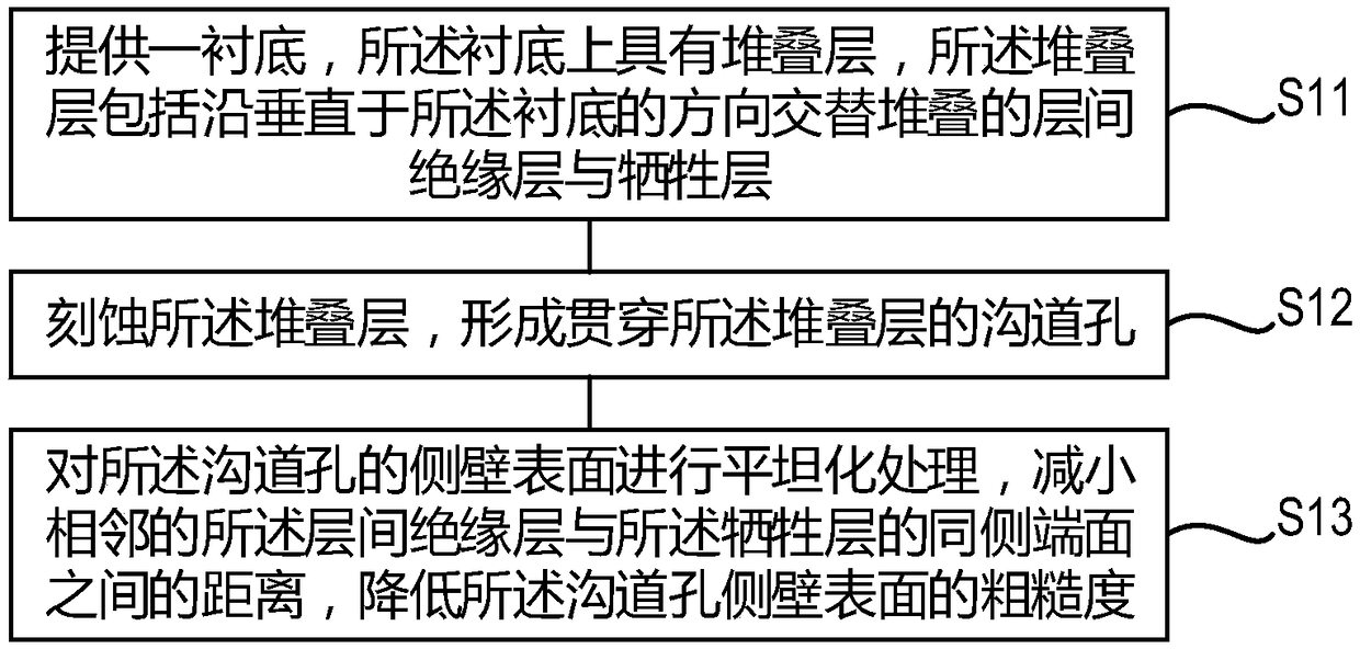
[0046] The manufacturing method of the three-dimensional memory and the specific implementation of the three-dimensional memory provided by the present invention will be described in detail below in conjunction with the accompanying drawings.

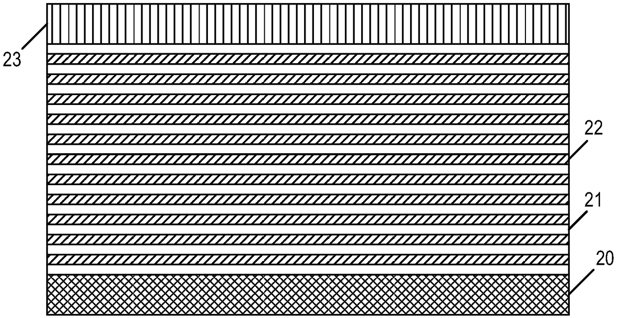
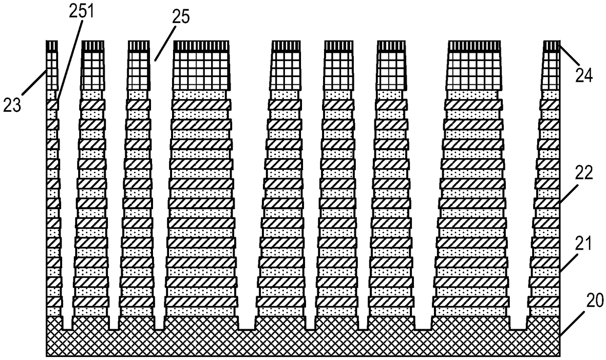
[0047] In the manufacturing process of a three-dimensional memory, firstly, a stacked layer composed of interlayer insulating layers and sacrificial layers stacked alternately along the direction perpendicular to the substrate is formed, and then formed by metallization steps A stack structure composed of stacked interlayer insulating layers and gate layers. Wherein, the metallization step refers to: removing the sacrificial layer in the stacked layers to form a gap region between adjacent interlayer insulating layers; and then filling the gap region with conductive material to form a gate layer. In order to realize the control of the memory cells, a channel hole penetrating through the stacked layers is formed through a dry etching pro...


PUM


Abstract

The invention relates to the technical field of semiconductor manufacturing, in particular to a manufacturing method of a three-dimensional memory and a three-dimensional memory. The manufacturing method of the three-dimensional memory comprises the following steps: providing a substrate having a stack layer on the substrate, the stack layer comprising an interlayer insulating layer and a sacrificial layer alternately stacked in a direction perpendicular to the substrate; Etching the stack layer to form a channel hole penetrating the stack layer. The sidewall surface of the channel hole is planarized to reduce the distance between the adjacent interlayer insulating layer and the same side end face of the sacrificial layer and to reduce the roughness of the sidewall of the channel hole. Theinvention reduces the roughness of the side wall surface of the channel hole, and remarkably improves the storage and erasing performance of the three-dimensional memory.

Description

technical field [0001] The invention relates to the technical field of semiconductor manufacturing, in particular to a method for manufacturing a three-dimensional memory and a three-dimensional memory. Background technique [0002] As technology develops, the semiconductor industry is constantly seeking new ways to produce a greater number of memory cells per memory die in a memory device. In non-volatile memory, such as NAND memory, one way to increase the memory density is by using vertical memory arrays, that is, 3D NAND (three-dimensional NAND) memory; 32 layers developed to 64 layers, or even higher layers. [0003] In a 3D NAND memory, there is a stack structure formed by alternately stacking interlayer insulating layers and gates, and the stack structure includes a core area and a stepped area surrounding the core area. The core area is used for storing information; the step area is located at the end of the stack structure and is used for transmitting control info...

Claims


Application Information

Patent Timeline
Patent Type & Authority Applications(China)
IPC IPC(8): H01L27/11551H01L27/11578
CPCH10B41/20H10B43/20
Inventor 肖莉红李君
Owner YANGTZE MEMORY TECH CO LTD
Why Eureka
Try Eureka