
Light-emitting diode assembly and manufacturing method thereof

A technology of light-emitting diodes and components, which is applied in the manufacture of semiconductor/solid-state devices, semiconductor devices of light-emitting elements, light sources, etc., and can solve the problems of time-consuming manufacturing process

Inactive Publication Date: 2019-01-25
EPISTAR CORP
View PDF5 Cites 0 Cited by
  • Summary
  • Abstract
  • Description
  • Claims
  • Application Information

AI Technical Summary

Problems solved by technology

[0005] However, the manufacturing process of removing the LED chips on the temporary carrier film one by one and fixing them in the base of an LED product is often very time-consuming

Method used


Image

  • Light-emitting diode assembly and manufacturing method thereof
  • Light-emitting diode assembly and manufacturing method thereof
  • Light-emitting diode assembly and manufacturing method thereof

Examples


Embodiment Construction

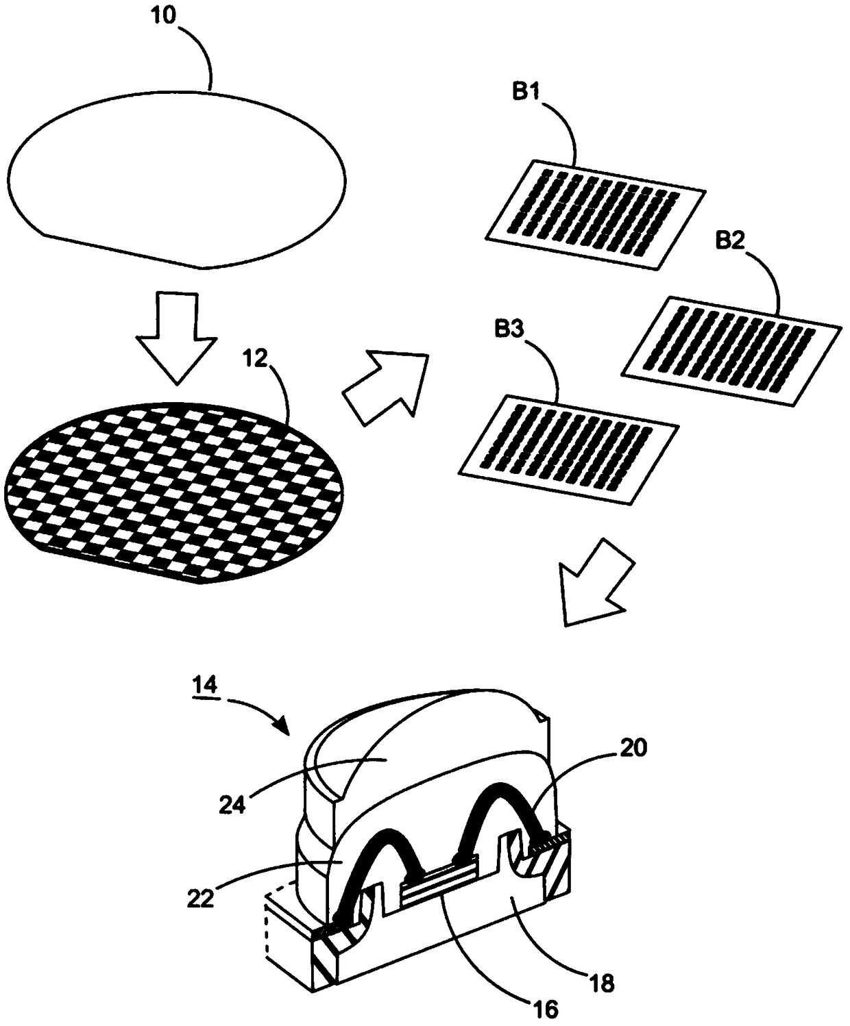
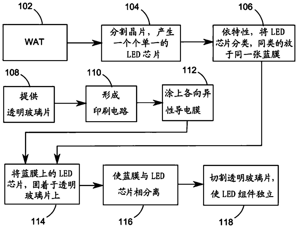
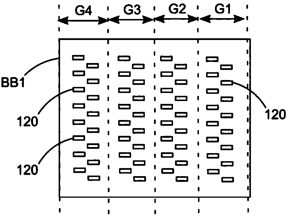
[0041] figure 2 It is a method for manufacturing an LED component according to the present invention. Step 102 performs a wafer acceptance test (WAT) on the wafer 12 with chips to determine whether it meets the specification. Step 104 cuts the qualified wafer 12 to separate individual LED chips. Step 106 detects each LED chip and classifies it according to its photoelectric characteristics, such as forward voltage, dominant wavelength, luminous intensity, etc., and classifies LED chips of the same type Placed on a temporary carrier film, the temporary carrier film can be blue tape. image 3 A temporary carrier film BB1 implemented according to the present invention is shown, on which LED chips 120 belonging to the same category are adhered. According to the positions, the LED chips 120 of the temporary carrier film BB1 can be roughly divided into four groups G1, G2, G3, and G4. The positions of all LED chips 120 in each group form a pattern, and the patterns of each group...


PUM


Abstract

The invention discloses a manufacturing method for an LED assembly. The manufacturing method includes providing a first carrier, wherein several LED chips are formed on the first carrier; providing asecond carrier; attaching the second carrier to the LED chips; and detaching the first carrier from the LED chips but leaving the LED chips on the second carrier.

Description

[0001] This application is a divisional application of the Chinese invention patent application (application number: 201410507456.7, application date: September 28, 2014, invention name: light-emitting diode component and manufacturing method). technical field [0002] The invention relates to a manufacturing method of a light emitting diode (LED) assembly. Background technique [0003] At present, we can already see the application of various LED products in daily life, such as traffic signs, motorcycle tail lights, car headlights, street lights, computer indicator lights, flashlights, LED backlights, etc. In addition to the chip manufacturing process, almost all of these products must go through the packaging process. [0004] figure 1 Shows a whole process of traditional LED components. Firstly, a sapphire substrate 10 is provided. Next, a plurality of LED chips (chips) are formed on the sapphire substrate 10 by using epitaxy, thin film, photolithography, etching and o...

Claims


Application Information

Patent Timeline
Patent Type & Authority Applications(China)
IPC IPC(8): F21K9/90H01L25/075H01L21/60
CPCH01L21/683H01L33/005F21K9/90H01L24/29H01L24/32H01L24/48H01L24/83H01L24/97H01L25/0753H01L2224/2929H01L2224/293H01L2224/32245H01L2224/48229H01L2224/48249H01L2224/73265H01L2224/83005H01L2224/83192H01L2224/83851H01L2224/83862H01L2224/9202H01L2224/97H01L2924/00014H01L2924/12041H01L2924/181H01L2933/0033H01L2924/00H01L2224/83H01L2924/00012H01L2224/45099H01L2224/45015H01L2924/207
Inventor 郑子淇
Owner EPISTAR CORP
Learn More