An optical detection system

A technology for optical detection and detection, which is applied in the direction of optical testing of flaws/defects, material analysis through optical means, and measuring devices. It can solve problems such as poor accuracy, outflow of defective products, and low efficiency, so as to improve detection efficiency and accuracy. The effect of reducing the probability of defective product outflow

Active Publication Date: 2021-02-19
NANTONG FUJITSU MICROELECTRONICS
View PDF2 Cites 0 Cited by
  • Summary
  • Abstract
  • Description
  • Claims
  • Application Information

AI Technical Summary

Problems solved by technology

[0004] The inventors of the present application found in the long-term research process that the above-mentioned existing macroscopic detection has the disadvantages of low efficiency and poor accuracy, and it is easy to cause defective products to flow out

Method used


Image

  • An optical detection system
  • An optical detection system
  • An optical detection system

Examples


Embodiment Construction

[0024] The following will clearly and completely describe the technical solutions in the embodiments of the present application with reference to the drawings in the embodiments of the present application. Obviously, the described embodiments are only some of the embodiments of the present application, not all of them. Based on the embodiments in this application, all other embodiments obtained by persons of ordinary skill in the art without making creative efforts belong to the scope of protection of this application.

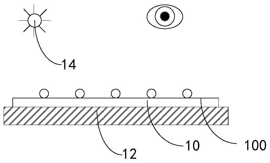
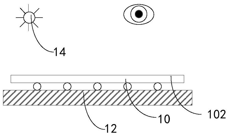
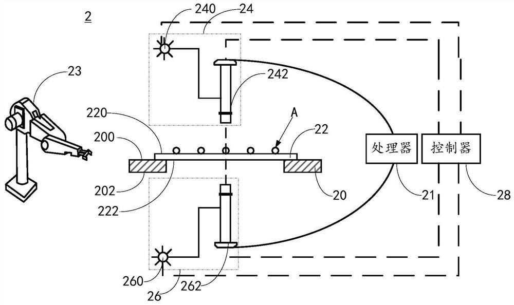
[0025] see figure 2 , figure 2 It is a schematic structural diagram of an embodiment of the optical detection system of the present application. The optical detection system 2 provided by the present application includes:

[0026] The base 20 includes a first surface 200 and a second surface 202 opposite to each other. The first surface 200 is used to carry the sample 22 to be detected. The material of the base 20 can be plastic, glass, silicon, etc., and ...


PUM


Abstract

The present application discloses an optical detection system. The optical detection system includes: a base platform, including a first surface and a second surface oppositely arranged, and the first surface is used to carry a sample to be detected; a first detection component and a The second detection component is respectively located on the side of the first surface and the second surface of the base platform, and the detection direction is respectively facing the first surface and the second surface of the base platform. , the first detection component is used to directly obtain a first image of the first surface of the sample to be detected, and the second detection component is used to obtain the opposite second surface of the sample to be detected through the base platform The second image of the sample to be inspected is combined with the first image and the second image of the sample to be inspected to determine whether there is a defect in the sample to be inspected. Through the above method, the present application can improve the efficiency and accuracy of defect detection.

Description

technical field [0001] The present application relates to the technical field of semiconductors, in particular to an optical detection system. Background technique [0002] Wafers, substrates, etc. commonly used in the semiconductor industry, all involve macroscopic inspection of the front and back of wafers or substrates during incoming material inspection, process and final shipment. [0003] For example, if Figure 1a and 1b as shown, Figure 1a It is a structural schematic diagram of an implementation mode of existing macro detection, Figure 1b It is a structural schematic diagram of another embodiment of the existing macro detection. The sample 10 to be inspected (for example, a wafer, a substrate, etc.) is placed on the base platform 12, and under the illumination of the light source 14, whether there is a defect (such as Figure 1a shown); then the sample 10 to be inspected is turned over, and whether there is a defect in the back 102 of the sample to be inspected ...

Claims


Application Information

Patent Timeline
Patent Type & Authority Patents(China)
IPC IPC(8): G01N21/88G01N21/01
CPCG01N21/01G01N21/88
Inventor 丁万春范伟
Owner NANTONG FUJITSU MICROELECTRONICS
Why Eureka
Try Eureka