
A variable pitch electronic component mass transfer device and method

A technology of electronic components and transfer devices, applied in the direction of electrical components, electrical components, electrical solid devices, etc., which can solve the problems of inability to ensure the yield rate of self-assembly

Active Publication Date: 2019-05-24
GUANGDONG UNIV OF TECH
View PDF4 Cites 0 Cited by
  • Summary
  • Abstract
  • Description
  • Claims
  • Application Information

AI Technical Summary

Problems solved by technology

However, this method has a certain randomness and cannot ensure the yield of self-assembly

Method used


Image

  • A variable pitch electronic component mass transfer device and method
  • A variable pitch electronic component mass transfer device and method
  • A variable pitch electronic component mass transfer device and method

Examples


Embodiment Construction

[0033] The technical solution of the present invention will be further described below in conjunction with the accompanying drawings and through specific implementation methods.

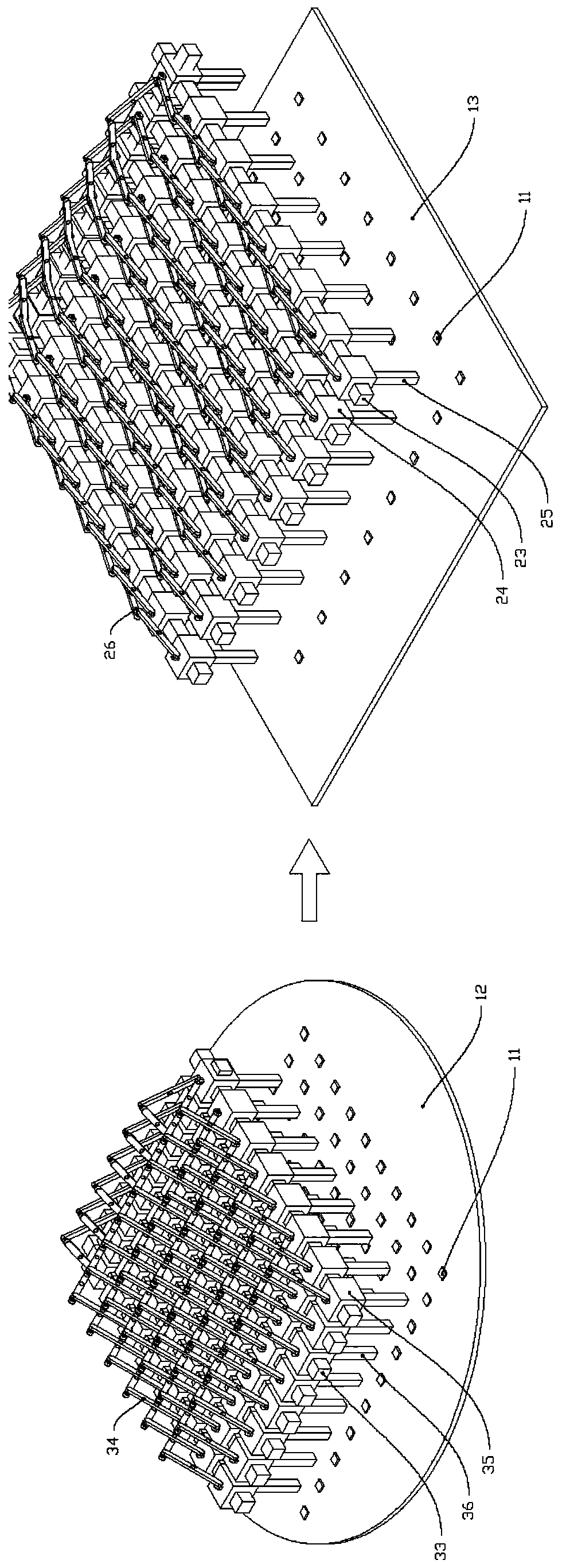
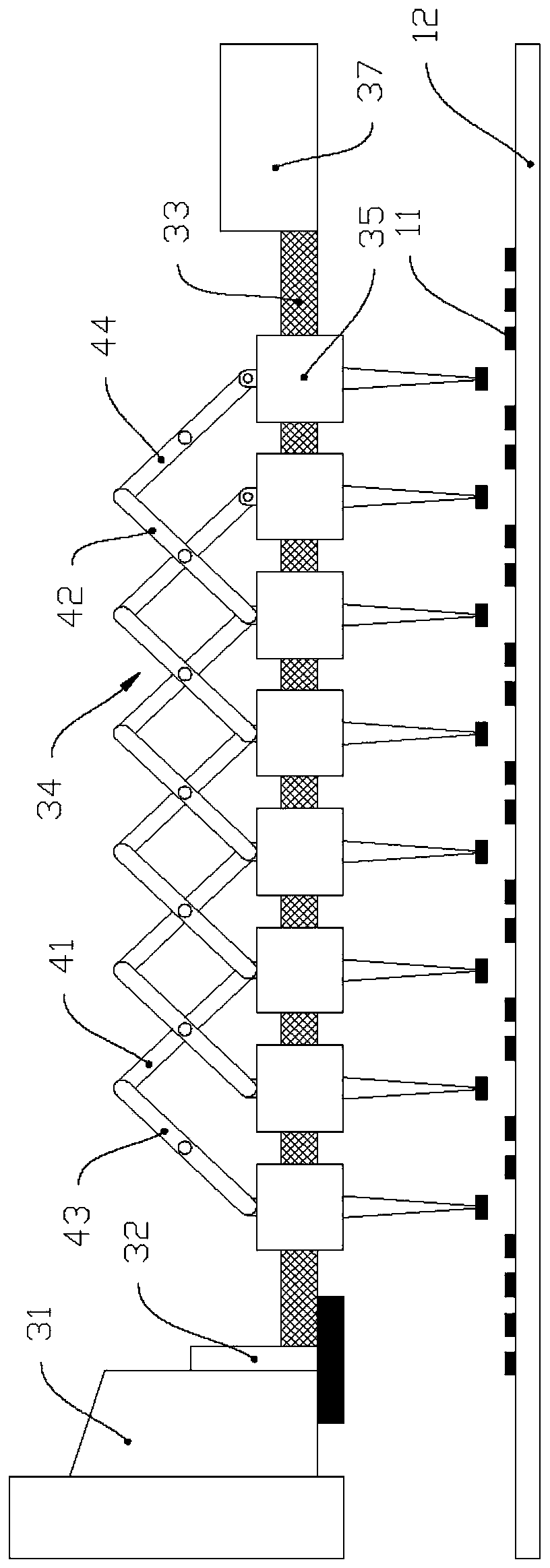
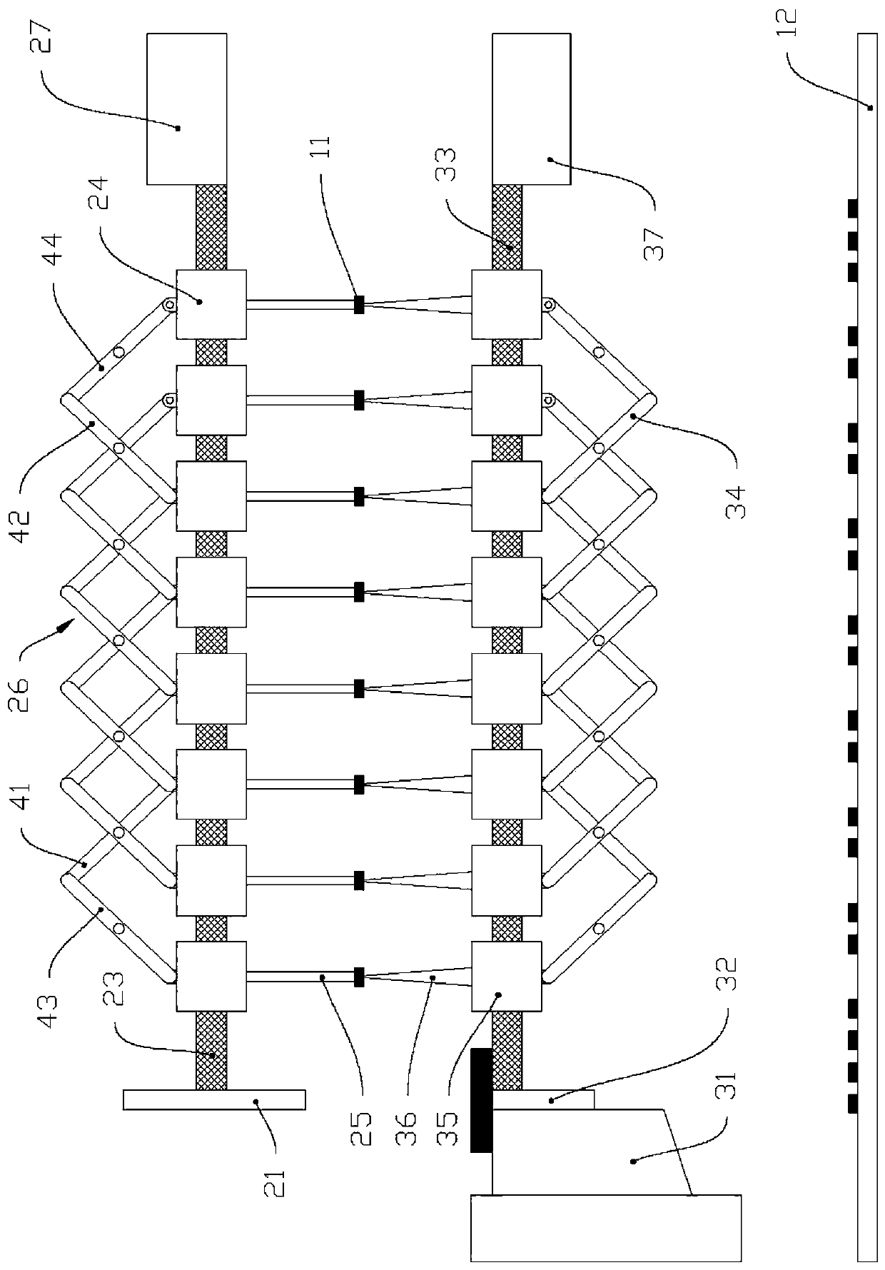
[0034] A mass transfer device for electronic components with variable pitch in this embodiment, such as Figure 2-4 As shown, including die bonding arm, die bonding drive motion platform, flip chip soldering arm, flip chip drive motion platform and operation table;

[0035] There are a plurality of said die-bonding arms, each of which includes a die-bonding guide rail 23, a die-bonding bracket 24, a crystal-bonding transfer head 25, a crystal-bonding connecting rod 26, and a crystal-bonding linear motor 27. There are a plurality of crystal-bonding brackets 24, and a plurality of the crystal-bonding brackets 24 are slidably connected with the described crystal-bonding guide rails 23, and each of the crystal-bonding brackets 24 is provided with a crystal-bonding transfer head 25 below. The crystal-bon...


PUM


Abstract

The invention discloses a large-volume transfer device for electronic components with variable spacing. A plurality of die-bonding brackets are slidingly connected with a die-bonding guide rail. The rods are equipped with equally spaced die-bonding movable nodes, and each die-bonding movable node is hinged to a die-bonding bracket. The die-bonding linear motor is set at one end of the die-bonding guide rail, and the output end of the die-bonding linear motor drives the die-bonding connecting rod. Telescopic movement; multiple flip-chip brackets are slidingly connected with the flip-chip guide rails, each flip-chip bracket is provided with a flip-chip transfer head, and the flip-chip connecting rods are equipped with flip-chip movable nodes arranged at equal intervals. The flip-chip movable node is hinged with a flip-chip bracket, the flip-chip linear motor is set at one end of the flip-chip guide rail, and the output end of the flip-chip linear motor drives the telescopic movement of the flip-chip connecting rod; The connection is used to turn over the flip-chip guide rail; the invention can realize mass transfer with fully controllable pitch of electronic components.

Description

technical field [0001] The invention relates to the field of novel semiconductor displays, in particular to a mass transfer device and method for variable-pitch electronic components. Background technique [0002] Micro-LED is a display technology that miniaturizes and matrixes the LED structure, and individually drives and addresses each pixel. Since the brightness, life, contrast, response time, energy consumption, viewing angle and resolution of Micro-LED technology are superior to LCD and OLED technology, it is regarded as a new generation of display technology that can surpass OLED and traditional LED. . However, due to the requirements of extremely high efficiency, 99.9999% yield and transfer accuracy within plus or minus 0.5 μm in the packaging process, the size of Micro-LED components is basically less than 50 μm and the number is tens of thousands to millions. Therefore, in Micro- A core technical problem that still needs to be overcome in the process of LED indus...

Claims


Application Information

Patent Timeline
Patent Type & Authority Patents(China)
IPC IPC(8): H01L21/67H01L33/48
CPCH01L33/48H01L21/67092H01L21/67144H01L2933/0033H01L33/0095H01L24/75H01L2224/7598H01L2924/12041H01L2224/757H01L2224/75702H01L2224/75725H01L2924/00012H05K13/0411H01L33/005H01L33/62H01L2933/0066H05K13/0465
Inventor 陈新贺云波麦锡全崔成强刘强张凯高健杨志军陈桪陈云汤晖张昱
Owner GUANGDONG UNIV OF TECH
Learn More