A method to achieve the uniformity of the brightness of the SEM image of the whole nanoparticle

A nanoparticle and image brightness technology, which is used in image enhancement, image analysis, image data processing, etc., can solve the problems of inability to achieve uniformity of the brightness of nanoparticle SEM images, and inability to achieve interpolation and correction of the border around the image.

Active Publication Date: 2021-02-19
HEBEI UNIV OF TECH +1
View PDF11 Cites 0 Cited by
  • Summary
  • Abstract
  • Description
  • Claims
  • Application Information

AI Technical Summary

Problems solved by technology

[0006] The technical problem to be solved by the present invention is to provide a method for realizing uniform brightness of the overall nanoparticle SEM image, which is to obtain the pixel value of the block equalization splicing image of the original image of the nanoparticle SEM and the symmetrical extension block equalization of the nanoparticle SEM. The average value of the image pixel value is intercepted by means of splicing to achieve uniform brightness of the overall nanoparticle SEM image, which overcomes the inability of the existing technology to use masking method, block processing, and division of regions only suitable for correction of non-edge parts of the image. Realize the interpolation and correction of the boundary part around the image, that is, the defect that the brightness of the overall nanoparticle SEM image cannot be uniformed

Method used


Image

  • A method to achieve the uniformity of the brightness of the SEM image of the whole nanoparticle
  • A method to achieve the uniformity of the brightness of the SEM image of the whole nanoparticle
  • A method to achieve the uniformity of the brightness of the SEM image of the whole nanoparticle

Examples


Embodiment 1

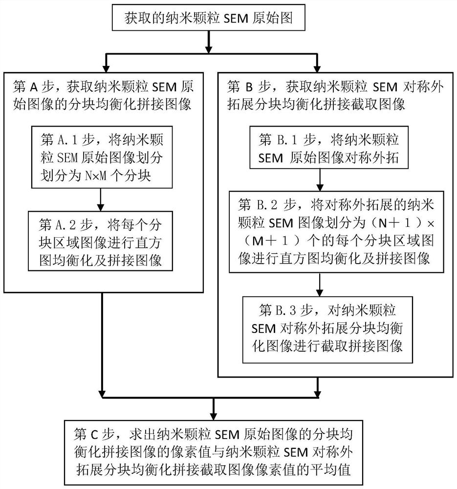
[0079] In this embodiment, the method for realizing uniform brightness of the overall nanoparticle SEM image, the specific steps are as follows:

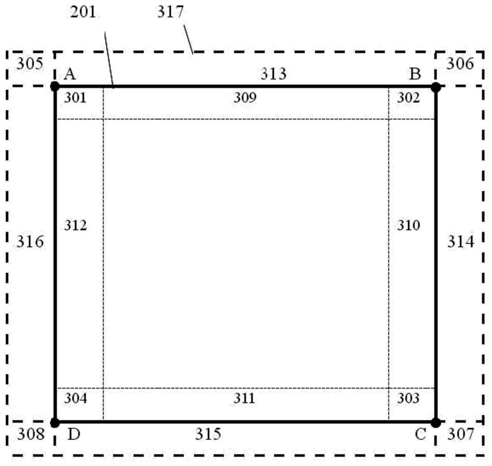
[0080] In step A, obtain the block-equalized mosaic image of the original nanoparticle SEM image:

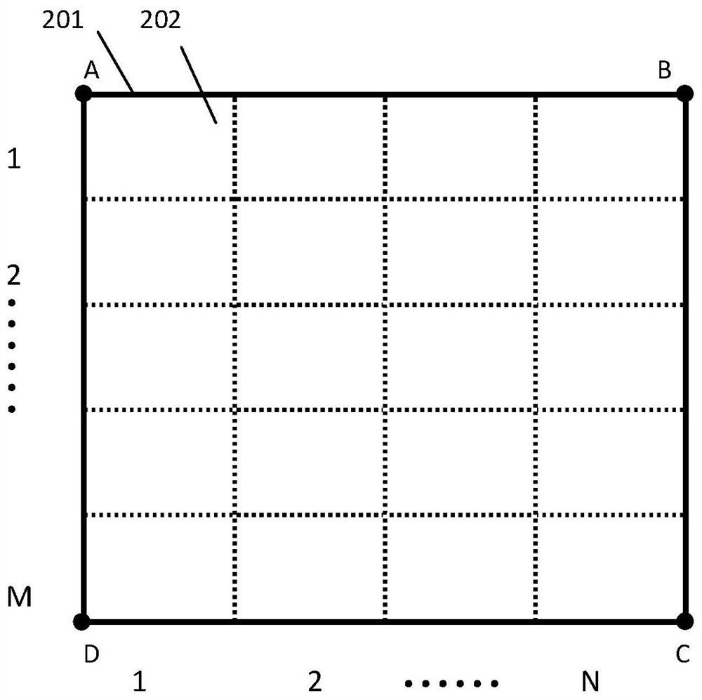
[0081] In the first step A.1, the original nanoparticle SEM image is divided into N×M block area images:

[0082] Divide the acquired nanoparticle SEM original image, that is, the entire nanoparticle SEM image with uneven brightness, into N×M block area images of horizontal N equal parts and vertical M equal parts, where N≥3, M≥3, except There is a common edge between adjacent blocks, and the blocks do not overlap with each other. A single block must contain at least ten nanoparticles. The horizontal width of each block is n pixels, and the vertical height is m pixels. Where n and m are even numbers, corresponding to the entire nanoparticle SEM image, with N×n pixels in the horizontal direction and M×m pixels in the vertical directio...


PUM


Abstract

A method for homogenizing that brightness of a whole nanoparticle SEM image relates to the image data processing using histogram techniques, and obtains the average value of the pixel value of the block equalization mosaic image of the nanometer particle SEM original image and the pixel value of the symmetrical outer expansion block equalization mosaic mosaic image of the nanometer particle SEM, and the average value of the pixel value of the block equalization mosaic mosaic image of the nanometer particle SEM original image, so that the brightness uniformity of the whole nano-particle SEM image is realized. The prior art adopts the mask method, the partition processing and the partition region are only adapted to the correction of the non-edge part of the image, the defect that the interpolation and correction of the boundary part around the image can not be realized, that is, the brightness uniformity of the whole nano-particle SEM image can not be realized.

Description

technical field [0001] The technical solution of the present invention relates to image data processing using the histogram technique, in particular to a method for realizing uniform brightness of the overall nanoparticle SEM image. Background technique [0002] Scanning Electron Microscope (Scanning Electron Microscope in English, hereinafter referred to as SEM), as a modern analytical instrument, is widely used in the microscopic fields of many disciplines in medicine, biology and materials, especially in recent years to characterize the surface micromorphology of nanoparticles. Research. [0003] The electron beam accelerated by the voltage is converged by the magnetic lens and scanned by the coil, and the surface morphology of the sample is observed by imaging the secondary electron signal. The scanning electron microscope can achieve ultra-high resolution at the nanometer level. Due to the long-time working of the electron microscope, the filament shifts and swings to ...

Claims


Application Information

Patent Timeline
Patent Type & Authority Patents(China)
IPC IPC(8): G06T5/00G06T5/40G06T5/50
CPCG06T5/005G06T5/40G06T5/50G06T2207/10061G06T2207/20216
Inventor 赵红东李宇海韩力英杨东旭马俊成康晴孙梅
Owner HEBEI UNIV OF TECH
Why Eureka
Try Eureka