Display panel

A display panel, substrate wiring technology, applied in static indicators, instruments, etc., can solve problems such as gate driver chips not being able to output, timing differences, etc.

Inactive Publication Date: 2019-03-12
HKC CORP LTD
View PDF13 Cites 0 Cited by
  • Summary
  • Abstract
  • Description
  • Claims
  • Application Information

AI Technical Summary

Problems solved by technology

[0003] However, due to the resistance of the substrate traces between the two gate driver chips
This will cause timing differences between the control signal received by the latt...

Method used


Image

  • Display panel
  • Display panel
  • Display panel

Examples


Embodiment Construction

[0042] In order to make the purpose, technical solution and advantages of the present application clearer, the present application will be further described in detail below in conjunction with the accompanying drawings and embodiments. It should be understood that the specific embodiments described here are only used to explain the present application, and are not intended to limit the present application.

[0043] The display panel provided by the present application can be applied to display devices such as computers, televisions, and other displays. The display type may be, but not limited to, a liquid crystal display, and may also be an organic light-emitting display or the like.

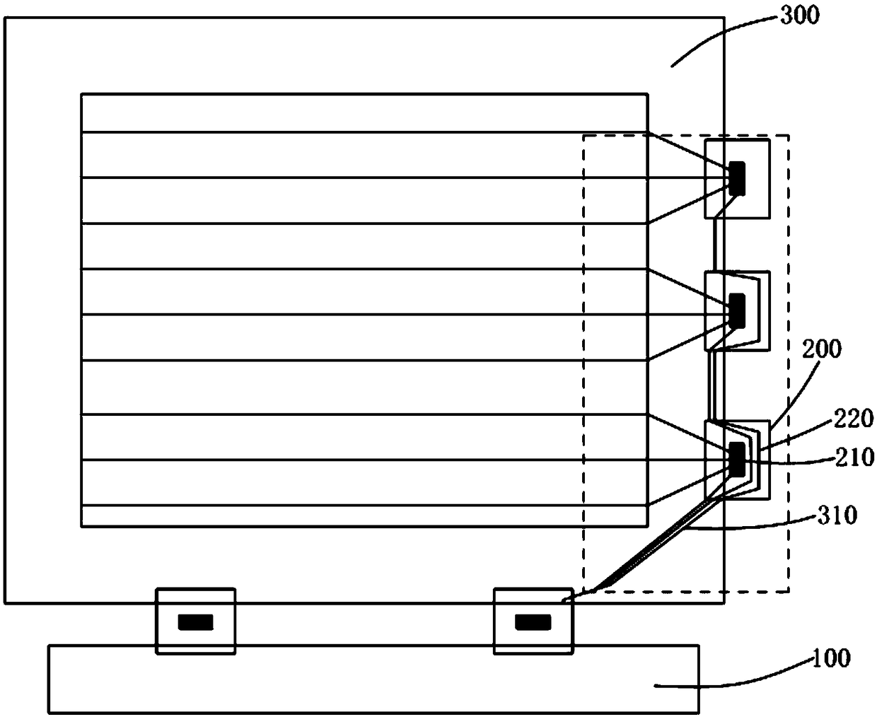
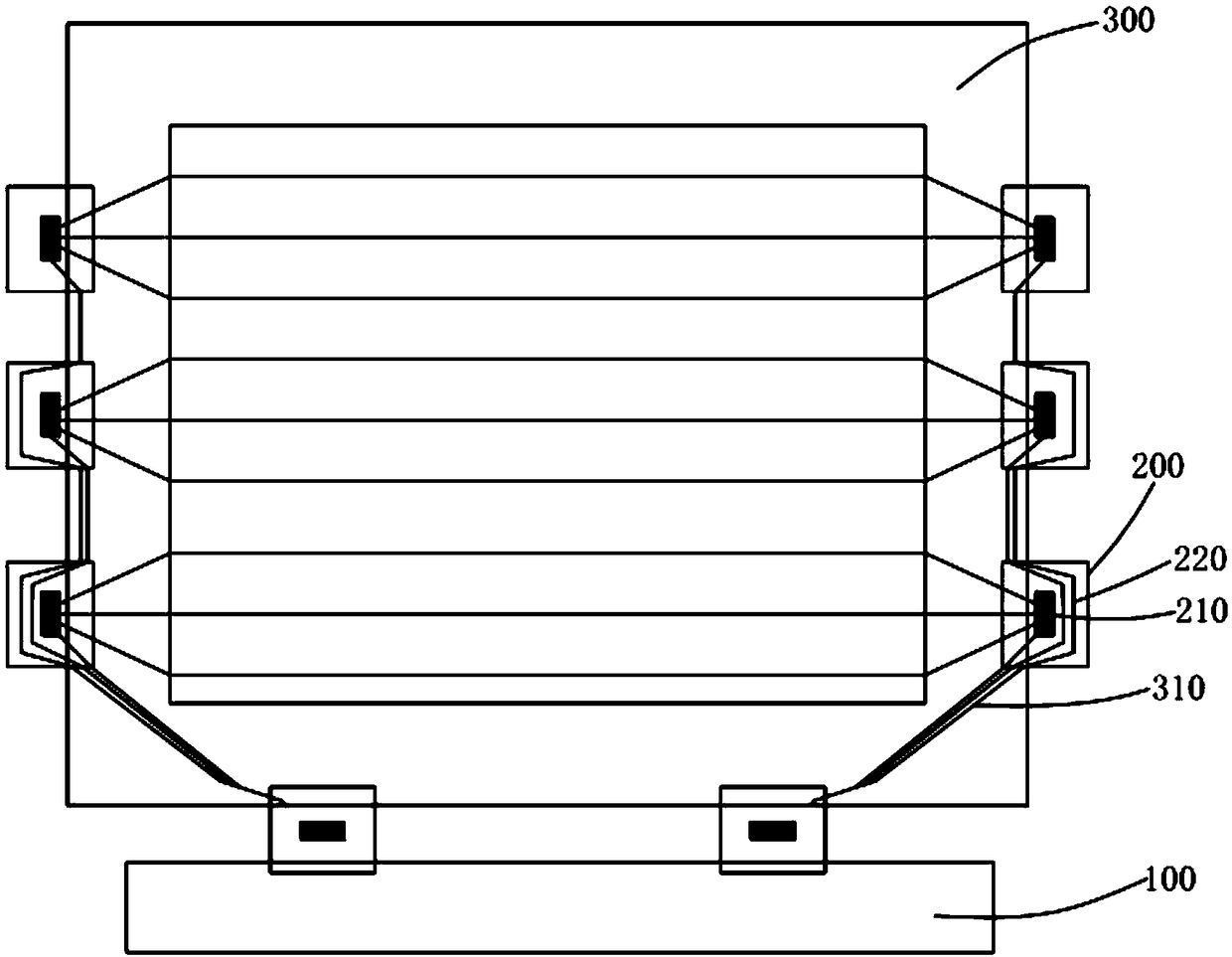
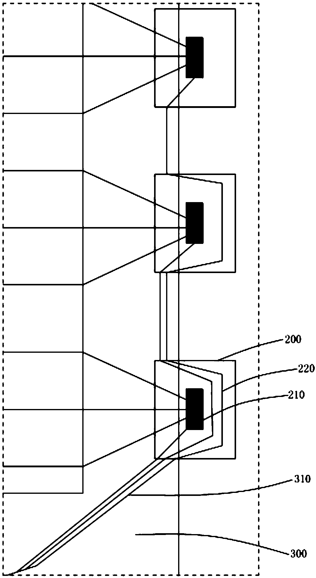
[0044] In one embodiment, refer to figure 1 , provides a display panel, including a control circuit board 100 , a gate driver chip 210 , and an array substrate 300 .

[0045] The control circuit board 100 may be an assembled printed circuit board (Printed Circuit Board+Assembly, PCBA). The co...


PUM


Abstract

The invention relates to a display panel. The display panel comprises a control circuit board, grid electrode driving chips and an array substrate. The array substrate comprises basic wires, and the basic wires are electrically connected with the control circuit board to form two or more signal transmission paths. The signal transmission paths are used for transmitting grid electrode control signals. The two or more grid electrode driving chips are electrically connected with different signal transmission paths, and the ratio of total resistance values of the basic wires between the two grid electrode driving chips electrically connected to different signal transmission paths and the control circuit board is a preset ratio. According to the display panel, at least the time sequence difference between the two grid electrode driving chips is improved, and the display accuracy of the display panel is improved.

Description

technical field [0001] The present application relates to the field of display technology, in particular to a display panel. Background technique [0002] With the development of display technology, the global display industry has maintained steady growth, and the trend of large screen sizes has driven the development of the industry. In medium and large size display panels, generally there are more than two gate driving chips for gate driving. In order to save costs, the drive control circuits of each gate drive chip are usually fabricated on one control circuit board. The control circuit board and the gate drive chips and the gate drive chips are connected to each other through substrate wires. The control signals of the control circuit board to each gate driver chip are transmitted through the wiring on the substrate. [0003] However, due to the resistance of the substrate wiring between the two gate drive chips. This will cause timing differences between the control...

Claims


Application Information

Patent Timeline
IPC IPC(8): G09G3/20G09G3/3266G09G3/3225G09G3/36
CPCG09G3/20G09G3/3225G09G3/3266G09G3/3677
Inventor 黄北洲
Owner HKC CORP LTD
Why Eureka
Try Eureka