An Electron Optical System

A technology of electron optics and incident electrons, which is applied in the field of electron optical systems, can solve problems such as low measurement efficiency, difficult adjustment of optical systems, and large aberrations, and achieve the effects of simple adjustment, small aberrations, and reduced aberrations

Active Publication Date: 2020-11-24
SHANGHAI INST OF MICROSYSTEM & INFORMATION TECH CHINESE ACAD OF SCI
View PDF6 Cites 0 Cited by
  • Summary
  • Abstract
  • Description
  • Claims
  • Application Information

AI Technical Summary

Problems solved by technology

[0006] In view of the shortcomings of the prior art described above, the object of the present invention is to provide an electron optical system, which can solve the problem of multi-channel electron spin analysis in the prior art when the electron optical system is used in a multi-channel electron spin analyzer. Problems such as low measurement efficiency, large aberration, and difficulty in debugging the optical system

Method used


Image

  • An Electron Optical System
  • An Electron Optical System
  • An Electron Optical System

Examples


Embodiment approach

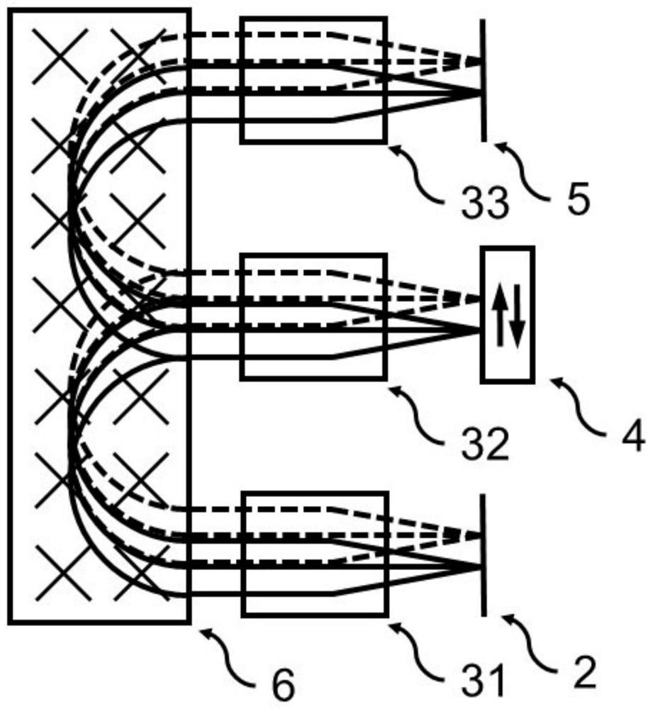
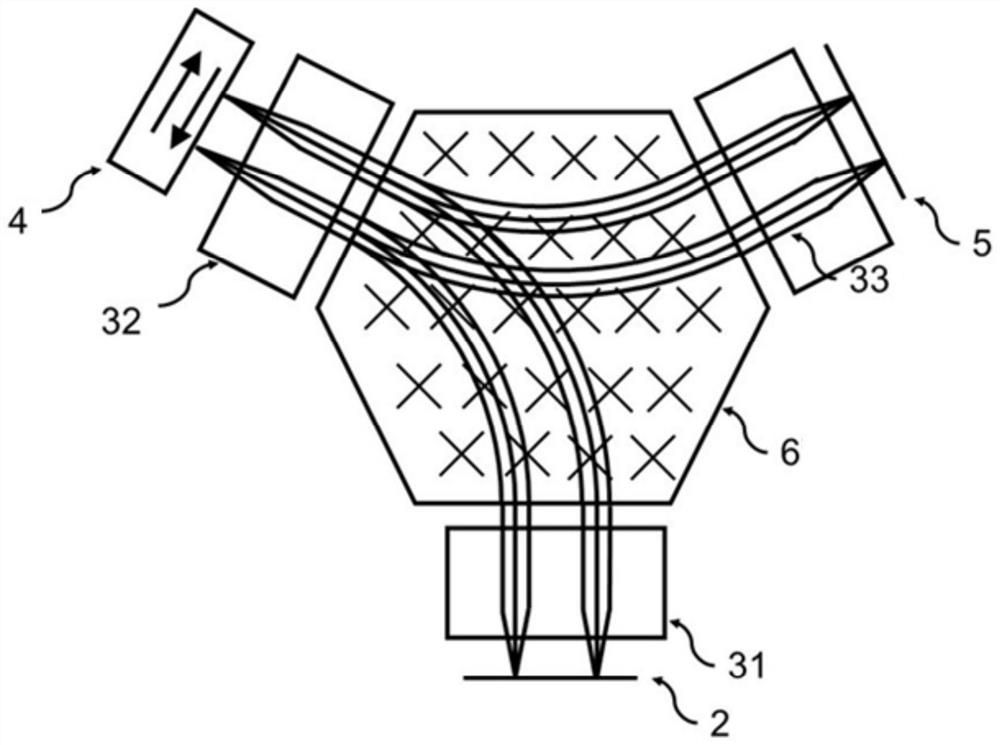
[0048] Specifically, the two-dimensional image-type electron detector 5 may be any device capable of recording electron intensity distribution. As an embodiment of the present invention, the two-dimensional image electron detector 5 is composed of a micro-channel plate (Micro-channel Plate, MCP), a fluorescent plate and a high-sensitivity camera. As another embodiment of the present invention, the two-dimensional image electron detector 5 is composed of a microchannel plate and a delay line detector (Delay Line Detector, DLD).

[0049] It should be noted that those skilled in the art should understand that the above description is only an example rather than a limitation to the present invention. In fact, any combination of a non-axisymmetric lens group and a magnetic field to bend the incident electron beam It is incident on the scattering target at an optimal incident angle and is imaged at a specific plane relative to the scattering target. At the same time, the outgoing el...


PUM


Abstract

An image-type electron spin analyser, comprising: an electron optical system, a scattering target (4) and a two-dimensional image-type electron detector (5), the electron optical system comprising a non-axisymmetric lens group and a magnetic field (6), the non-axisymmetric lens group being matched with the magnetic field (6) to enable movement tracks of incoming electrons and outgoing electrons to be mutually separated in order to increase the geometric degree of freedom of various parts of the spin analyser. The incoming electrons are deflected and imaged to a specific plane corresponding to the scattering target (4), and the electrons are imaged to the two-dimensional image-type electron detector (5), after being scattered by the scattering target (4), to form a two-dimensional electron intensity image, thereby implementing multi-channel measurement of electron spin. The introduction of non-axisymmetric lenses compensates for the asymmetry of electron optical properties of the magnetic field (6) on vertical and parallel magnetic field directions, reduces optical system aberrations, and enables electron optical system debugging to be simpler.

Description

[0001] This application is a divisional application for a patent with an application date of September 7, 2017, an application number of 201710800610.3, and an invention name of an image-type electron spin analyzer. technical field [0002] The invention relates to the technical field of electron spin analysis, in particular to an electron optical system. Background technique [0003] At present, analyzers for measuring electron spin mainly include Mott type, Spin-LEED type, and VLEED type analyzers. Among them, the measurement method of the Mott-type analyzer is: first accelerate the electrons to a kinetic energy of 20-100KeV, and then make the electrons scatter on a target with a high spin-orbit interaction material (usually composed of high atomic number elements), by measuring the scattered electrons The spin of the incident electron is measured by the asymmetry of the intensity; the Spin-LEED analyzer measures the intensity of the diffraction spot of the electron on the...

Claims


Application Information

Patent Timeline
Patent Type & Authority Patents(China)
IPC IPC(8): G01N24/00
CPCG01N24/00G01T1/32
Inventor 乔山
Owner SHANGHAI INST OF MICROSYSTEM & INFORMATION TECH CHINESE ACAD OF SCI
Why Eureka
Try Eureka